


EXTERNAL BUS
14-4
14.2.2
Bus Signal Types
Bus signals consist of three groups: address/data, control/status and bus arbitration. They are listed
in
Table 14.1
. Refer to
Section 1.4, “Related Documents” (pg. 1-10)
. A detailed description of all
signals can be found in these documents.
14.2.2.1
Clock Signal
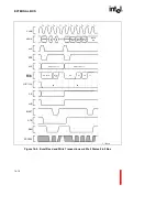
The CLKIN input signal is the reference for all i960 Jx microprocessor signal timing relationships.
Note that this is true even for the i960 JD processor, even though the CPU core runs at twice the
CLKIN rate. Transitions on the AD31:2, AD1:0, A3:2, ADS, BE3:0, WIDTH/HLTD1:0, D/C,
W/R, DEN, BLAST, RDYRCV, LOCK/ONCE, HOLD/HOLDA and BSTAT bus signal pins are
always measured directly from the rising edge of CLKIN. The processor asserts ALE and ALE
directly from the rising CLKIN edge at the beginning of a Ta state but deasserts them approxi-
mately half way through the state instead of the next rising CLKIN edge. All transitions on DT/R
are also referenced to a point halfway through the Ta state instead of rising CLKIN edges.
14.2.2.2
Address/Data Signal Definitions
The address/data signal group consists of 34 lines. 32 of these signals multiplex within the
processor to serve a dual purpose. During Ta, the processor drives AD31:2 with the address of the
bus access. At all other times, these lines are defined to contain data. A3:2 are demultiplexed
address pins providing incrementing word addresses during burst cycles. AD1:0 denote burst size
during Ta and data during other states.
The processor routinely performs data transfers less than 32 bits wide. If the programmed bus
width is 32 bits and transfers are 16- or 8-bit, then during write cycles the processor will replicate
the data that is being driven on the unused address/data pins. If the programmed bus width is 16 or
8 bits, then during write cycles the processor continues driving the previous address on any unused
address/data pins.
Whenever the programmed bus width is less than 32 bits, additional demultiplexed address bits are
available on unused byte enable pins (See
section 14.2.3.1, “Bus Width” (pg. 14-7)
). These signals
increment during burst accesses in similar fashion to the A3:2 pins.
14.2.2.3
Control/Status Signal Definitions
The control/status signal group consists of 15 signals. These signals control data buffers and
address latches or furnish information useful to external chip-select generation logic. All output
control/status signals are three-state.
Summary of Contents for i960 Jx
Page 1: ...Release Date December 1997 Order Number 272483 002 i960 Jx Microprocessor Developer s Manual ...
Page 24: ......
Page 25: ...1 INTRODUCTION ...
Page 26: ......
Page 35: ...2 DATA TYPES AND MEMORY ADDRESSING MODES ...
Page 36: ......
Page 46: ......
Page 47: ...3 PROGRAMMING ENVIRONMENT ...
Page 48: ......
Page 73: ...4 CACHE AND ON CHIP DATA RAM ...
Page 74: ......
Page 85: ...5 INSTRUCTION SET OVERVIEW ...
Page 86: ......
Page 111: ...6 INSTRUCTION SET REFERENCE ...
Page 112: ......
Page 233: ...7 PROCEDURE CALLS ...
Page 234: ......
Page 256: ......
Page 257: ...8 FAULTS ...
Page 258: ......
Page 291: ...9 TRACING AND DEBUGGING ...
Page 292: ......
Page 309: ...10 TIMERS ...
Page 310: ......
Page 324: ......
Page 325: ...11 INTERRUPTS ...
Page 326: ......
Page 369: ...12 INITIALIZATION AND SYSTEM REQUIREMENTS ...
Page 370: ......
Page 412: ......
Page 413: ...13 MEMORY CONFIGURATION ...
Page 414: ......
Page 429: ...14 EXTERNAL BUS ...
Page 430: ......
Page 468: ......
Page 469: ...15 TEST FEATURES ...
Page 470: ......
Page 493: ...A CONSIDERATIONS FOR WRITING PORTABLE CODE ...
Page 494: ......
Page 502: ......
Page 503: ...B OPCODES AND EXECUTION TIMES ...
Page 504: ......
Page 515: ...C MACHINE LEVEL INSTRUCTION FORMATS ...
Page 516: ......
Page 523: ...D REGISTER AND DATA STRUCTURES ...
Page 524: ......
Page 550: ......
Page 551: ...GLOSSARY ...
Page 552: ......
Page 561: ...INDEX ...
Page 562: ......
Page 578: ......