


TIMERS
10-6
10.1.1.5
Bits 4, 5 - Timer Input Clock Select (TMRx.csel1:0)
User software programs the TMRx.csel bits to select the Timer Clock (TCLOCK) frequency. See
Table 10-3
. As shown in
Figure 10-1
, the bus clock is an input to the timer clock unit. These bits
allow the application to specify whether TCLOCK runs at or slower than the bus clock frequency.
The processor clears these bits upon hardware or software reset (TCLOCK = Bus Clock).
10.1.2
Timer Count Register (TCR0, TCR1)
The Timer Count Register (TCRx) is a 32-bit register that contains the timer’s current count. The
register value decrements with each timer clock tick. When this register value decrements to zero
(terminal count), a timer interrupt is generated. When TMRx.reload is not set for the timer, the
status bit in the timer mode register (TMRx.tc) is set and remains set until the TMRx register is
accessed.
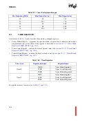
Figure 10-3
shows the timer count register.
Figure 10-3. Timer Count Register (TCR0, TCR1)
The valid programmable range is from 1H to FFFF FFFFH. (Avoid programming TCRx to 0 as it
has varying results as described in
section 10.5, “UNCOMMON TCRX AND TRRX
CONDITIONS” (pg. 10-12)
.)
User software can read or write TCRx whether the timer is running or stopped. Bit 3 of TMRx
determines user read/write control (see
section 10.1.1.4
). The TCRx value is undefined after
hardware or software reset.
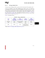
Table 10-3. Timer Input Clock (TCLOCK) Frequency Selection
Bit 5
TMRx.csel1
Bit 4
TMRx.csel0
Timer Clock (TCLOCK)
0
0
Timer Clock = Bus Clock
0
1
Timer Clock = Bus Clock / 2
1
0
Timer Clock = Bus Clock / 4
1
1
Timer Clock = Bus Clock / 8
28
24
20
4
0
16
12
8
Timer Count Register (TCR0, TCR1)
Timer Count Value - TCRx.d31:0
D31:0
Summary of Contents for i960 Jx
Page 1: ...Release Date December 1997 Order Number 272483 002 i960 Jx Microprocessor Developer s Manual ...
Page 24: ......
Page 25: ...1 INTRODUCTION ...
Page 26: ......
Page 35: ...2 DATA TYPES AND MEMORY ADDRESSING MODES ...
Page 36: ......
Page 46: ......
Page 47: ...3 PROGRAMMING ENVIRONMENT ...
Page 48: ......
Page 73: ...4 CACHE AND ON CHIP DATA RAM ...
Page 74: ......
Page 85: ...5 INSTRUCTION SET OVERVIEW ...
Page 86: ......
Page 111: ...6 INSTRUCTION SET REFERENCE ...
Page 112: ......
Page 233: ...7 PROCEDURE CALLS ...
Page 234: ......
Page 256: ......
Page 257: ...8 FAULTS ...
Page 258: ......
Page 291: ...9 TRACING AND DEBUGGING ...
Page 292: ......
Page 309: ...10 TIMERS ...
Page 310: ......
Page 324: ......
Page 325: ...11 INTERRUPTS ...
Page 326: ......
Page 369: ...12 INITIALIZATION AND SYSTEM REQUIREMENTS ...
Page 370: ......
Page 412: ......
Page 413: ...13 MEMORY CONFIGURATION ...
Page 414: ......
Page 429: ...14 EXTERNAL BUS ...
Page 430: ......
Page 468: ......
Page 469: ...15 TEST FEATURES ...
Page 470: ......
Page 493: ...A CONSIDERATIONS FOR WRITING PORTABLE CODE ...
Page 494: ......
Page 502: ......
Page 503: ...B OPCODES AND EXECUTION TIMES ...
Page 504: ......
Page 515: ...C MACHINE LEVEL INSTRUCTION FORMATS ...
Page 516: ......
Page 523: ...D REGISTER AND DATA STRUCTURES ...
Page 524: ......
Page 550: ......
Page 551: ...GLOSSARY ...
Page 552: ......
Page 561: ...INDEX ...
Page 562: ......
Page 578: ......