


UG-1262
Rev. B | Page 99 of 312
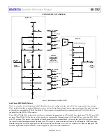
LPDAC0 CONTROL REGISTER
Address: 0x400C2128, Reset: 0x00000002, Name: LPDACCON0
Table 115. Bit Descriptions for LPDACCON0
Bits Bit
Name Settings
Description
Reset
Access
[31:7] Reserved
Reserved.
0x0
R
6
WAVETYPE
Low Power DAC Source.
0x0
R/W
0
Direct from the LPDACDAT0 register.
1
Waveform
generator.
5
DACMDE
LPDAC0 Switch Settings. Control bit for LPDAC0 output switches.
0x0
R/W
0
LPDAC0 switches set for normal mode. Clear to 0 for normal output switch
operation. Default.
1
LPDAC0 switches set for diagnostic mode.
4 VZEROMUX
VZERO0 Mux Select. Select which DAC0 output connects to the VZERO0 node.
Ensure that the same value is written to LPDACCON0, Bit 3 = 1. If this bit is cleared to
0, VBIASMUX must be cleared to 0.
0x0 R/W
0
VZERO0 6-bit. Default. Clear to 0 for VZERO0 output to be 6-bit.
1
VZERO0 12-bit. Set to 1 for VZERO0 output to be 12-bit.
3 VBIASMUX
VBIAS Mux Select. Select which DAC0 output connects to the VBIAS0 node. Ensure
that the same value is written to LPDACCON, Bit 4. If this bit is set to 1, the
VZEROMUX bit must be set to 1. If this bit is cleared to 0, VZEROMUX bit must be
cleared to 0.
0x0 R/W
0
VBIAS0 12-bit. Default. 12-bit DAC connect to VBIAS0.
1
VBIAS0 6-bit. 6-bit DAC connect to VBIAS0.
2
REFSEL
LPDAC0 Reference Select.
0x0
R/W
0
VREF_2.5V Reference 0. Selects the low power 2.5 V reference as the LPDAC0
reference source. Default.
1
AVDD Reference 1. Set to 1 to select AVDD as the low power DAC0 reference.
1
PWDEN
LPDAC0 Power-Down. Power-down control bit for low power DAC.
0x1
R/W
0
LPDAC0 powered on. Power on LPDAC0.
1
LPDAC0 powered off. Default. Power down LPDAC0 to open all switches on LPDAC0
output.
0
RSTEN
Enable Writes to LPDAC0. Enables writes to LPDACDAT0 register.
0x0
R/W
0
Disable LPDAC0 writes. Default. If cleared to 0, LPDACDAT0 is always 0. Writes to
LPDACDAT0 are disabled.
1
Enable LPDAC0 writes. Set to 1 to enable writes to the LPDACDAT0 register.
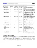
LPDAC1 DATA OUT REGISTER
Address: 0x400C212C, Reset: 0x00000000, Name: LPDACDAT1
Table 116. Bit Descriptions for LPDACDAT1
Bits Bit
Name
Settings
Description
Reset
Access
[31:18] Reserved
Reserved.
0x0 R
[17:12] DACIN6
6-Bit Value, 1 LSB = 34.375 mV. A low power DAC1 6-bit output data register values
between 0 and 0x3F is expected to set 6-bit output voltage.
0x0 R/W
000000
0.2
V.
111111
2.366
V.
[11:0] DACIN12
12-Bit Value, 1 LSB = 537 μV. A low power DAC1 12-bit output data register value
between 0 and 0xFFF is expected to set 12-bit output voltage.
0x0 R/W
0x000
0.2
V.
0xFFF
2.4
V.


