


UG-1262
Rev. B | Page 97 of 312
Bits
Bit
Name Settings Description
Reset Access
1 PAPDEN
Potentiostat Amplifier Power-Down. Low power Potentiostat Amplifier 1 power-down
control bit.
0x1 R/W
0
Power-up.
1
Power-down.
0
TIAPDEN
TIA Power-Down. Low power TIA1 power-down control bit.
0x1
R/W
0
Power
up.
1
Power
down.
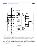
LOW POWER TIA SWITCH CONFIGURATION FOR CHANNEL 1 REGISTER
Address: 0x400C20E0, Reset: 0x00000000, Name: LPTIASW1
See Figure 17 for details on the switches mentioned in this register.
Table 112. Bit Descriptions for LPTIASW1
Bits Bit
Name Settings
Description
Reset
Access
[31:14] Reserved
Reserved.
0x0
R
13
TIABIASSEL
TIA SW13 Control Active High.
0x0
R/W
0
Disconnect TIA bias voltage from the VZERO0 pin.
1
Connect TIA bias voltage to the VZERO0 pin.
12
PABIASSEL
TIA SW12 Control Active High.
0x0
R/W
0
Disconnect potentiostat amplifier bias voltage from the VBIAS1 pin.
1
Connect potentiostat amplifier bias voltage to the VBIAS1 pin.
11
SW11
SW11 Switch Control Active High.
0x0
R/W
0
Open
switch.
1
Close
switch.
10
SW10
SW10 Switch Control Active High.
0x0
R/W
0
Open
switch.
1
Close
switch.
9
SW9
SW9 Switch Control Active High.
0x0
R/W
0
Open
switch.
1
Close
switch.
8
SW8
SW8 Switch Control Active High.
0x0
R/W
0
Open
switch.
1
Close
switch.
7
SW7
SW7 Switch Control Active High.
0x0
R/W
0
Open
switch.
1
Close
switch.
6
SW6
SW6 Switch Control Active High.
0x0
R/W
0
Open
switch.
1
Close
switch.
5 SW5
SW5 Switch Control Active High. Close to connect external capacitor or R
TIA
resistor
between the RC1_0 and RC1_1 pins.
0x0 R/W
0
Open
switch.
1
Close
switch.
4
SW4
SW4 Switch Control Active High.
0x0
R/W
0
Open
switch.
1
Close
switch.
3
SW3
SW3 Switch Control Active High.
0x0
R/W
0
Open
switch.
1
Close
switch.


