


UG-1262
Rev. B | Page 101 of 312
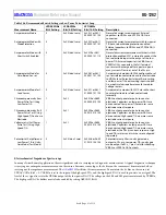
Bits Bit
Name Settings
Description
Reset
Access
1
PWDEN
Low Power DAC1 Power. Power-down control bit for low power DAC1.
0x1
R/W
0
Low Power DAC1 powered on. Clear to 0 to power on low power DAC1.
1
Low Power DAC1 powered off. Default. Power down low power DAC1 and open all
switches on the low power DAC1 output.
0
RSTEN
Enable Writes to LPDACDAT1.
0x0
R/W
0
Disable low power DAC1 writes. Default. If cleared to 0, LPDACDAT1 is always 0.
Writes to LPDACDAT1 are disabled.
1
Enable low power DAC1 writes.
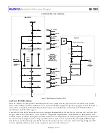
LOW POWER REFERENCE CONTROL REGISTER
Address: 0x400C2050, Reset: 0x00000000, Name: LPREFBUFCON
Table 119. Bit Descriptions for LPREFBUFCON
Bits Bit
Name
Settings Description
Reset Access
[31:3] Reserved
Reserved.
0x0
R
2
BOOSTCURRENT
Set this Bit when Using both Channel 0 and Channel 1 Potentiostat Channels.
0x0
R/W
0
Option to clear to 0 when using only one potentiostat channel to support only
one low power DAC and save power.
1
Set to 1 to boost bias current of low power reference buffer to support driving
two low power DACs.
1 LPBUF2P6DIS
Low Power Band Gap Output Buffer. Normally cleared to enable the low power
reference buffer.
0x0 R/W
0
Enable low power 2.5 V buffer.
1
Power down low power 2.5 V buffer.
0 LPREFDIS
Low Power Band Gap Power-Down Bit. Normally cleared to enable the low
power reference.
0x0 R/W
0
Low power reference enabled.
1
Low power reference powered down.


