


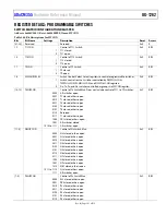


UG-1262
Rev. B | Page 130 of 312
SEQUENCER
SEQUENCER FEATURES
The features of the
sequencer are as follows:
Programmable for cycle accurate applications.
Four separate command sequences.
6 kB SRAM to store sequences.
FIFO to store measurement results.
Control via the wake-up timer or direct register write.
Various interrupts from user maskable sources.
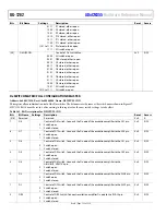
SEQUENCER OVERVIEW
The role of the sequencer is to allow offloading of the low level AFE operations from the digital die and to provide cyclic accurate control
over the analog DSP blocks. The sequencer handles timing critical operations without being subject to system load.
Four command sequences are supported by hardware on the
. These sequences can be stored in the SRAM to switch between
different measurement procedures. Only one sequence can be executed by the sequencer at a time. However, the user can configure
which sequences the sequencer executes and the order in which they are executed.
The sequencer reads commands from the sequence that is stored in the command memory and, depending on the command, either
waits a certain amount of time or writes a value to an MMR. The execution is sequential with no branching. The sequencer cannot read
MMR values or signals from the analog or DSP blocks.
To enable the sequencer, set the SEQEN bit in the SEQCON register. To disable the sequencer, write 0 to this bit.
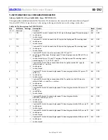
The rate at which the sequencer commands are executed is provided in the SEQWRTMR bits in the SEQCON register. When a write
command is executed by the sequencer, the sequencer performs the MMR write and then waits SEQWRTMR clock cycles before fetching the
next command in the sequence. The effect is the same as a write command followed by a wait command. The main purpose of this setup
is to reduce code size when generating arbitrary waveforms. The SEQWRTMR bits do not have any effect following a wait or timeout command.
In addition to a single write command being followed by a wait command, multiple write commands can be executed in succession followed
by a wait command. Any configuration can be rapidly set up by the sequencer, regardless of the number of register writes followed by a
precisely executed delay.
The sequencer can also be paused by setting the SEQHALT bit in the SEQCON register. This option applies to each function, including
FIFO operations, internal timers, and waveform generation. Reads from the MMRs are allowed when the sequencer is paused. This mode
is intended for debugging during software development.
The number of commands executed by the sequencer can be read from the SEQCNT register. Each time a command is read from command
memory and executed, the counter increments by 1. To reset the counter, perform a write to the SEQCNT register.
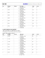
The sequencer calculates the cyclic redundancy check (CRC) of all commands it executes. The algorithm used is the CRC-8, using the x
8
+
x
2
+ x + 1 polynomial. The CRC-8 algorithm performs on 32-bit input data (sequencer instructions). Each 32-bit input is processed in one
clock cycle and the result is available immediately for reading by the host controller. The CRC value can be read from the SEQCRC register. To
reset this register by the same mechanism as the command count, write to the SEQCNT register. The SEQCRC register resets to a seed
value of 0x01. SEQCRC is a read only register.
SEQUENCER COMMANDS
Two types of commands can be executed by the sequencer: write commands and timer commands, which include wait commands and
timeout commands.
Write Command
Use a write instruction to write data to a register. The register address must lie between 0x400C0000 and 0x400C21FC. Figure 28 shows the
format of the instruction. The MSB is equal to 1, which indicates a write command.
In Figure 28, ADDR is the write address and data is the write data to be written to the MMR. All write instructions finish within one cycle.
The address field is seven bits wide to allow access to registers from Address 0x0 to Address 0x1FC in the AFE register block. All MMR
accesses are 32 bits. Byte and half word accesses are forbidden. All accesses are write only. There is a direct mapping between the address
field and the MMR address. In Figure 28, ADDR corresponds to Bits[8:2] of the 16-bit MMR address.


