


UG-1262
Rev. B | Page 263 of 312
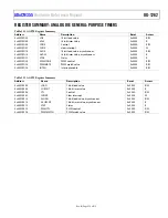
Bits Bit
Name
Settings
Description
Reset Access
1
OE
Overrun Error. If set, this bit self clears after COMLSR is read.
0x0
RC
0
Receive data has not been overwritten.
1
Receive data was overwritten by new data before COMRX was read.
0
DR
Data Ready. This bit is cleared only by reading COMRX. If set, this bit does not self clear.
0x0
RC
0
COMRX does not contain new receive data.
1
COMRX contains receive data that needs to be read.
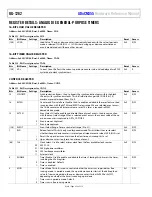
MODEM STATUS REGISTER
Address: 0x40005018, Reset: 0x0000, Name: COMMSR
Table 328. Bit Descriptions for COMMSR
Bits Bit
Name
Settings
Description
Reset
Access
[15:4] Reserved
Reserved.
0x0 R
3
DDCD
Delta DCD. If set, this bit self clears after COMMSR is read.
0x0
R
0
DCD has not changed state since COMMSR was last read.
1
DCD changed state since COMMSR was last read.
2
TERI
Trailing Edge Ring Indicator. If set, this bit self clears after COMMSR is read.
0x0
R
0
RI has not changed from 0 to 1 since COMMSR was last read.
1
RI changed from 0 to 1 since COMMSR was last read.
1
DDSR
Delta DSR. If set, this bit self clears after COMMSR is read.
0x0
R
0
DSR has not changed state since COMMSR was last read.
1
DSR changed state since COMMSR was last read.
0
DCTS
Delta CTS. If set, this bit self clears after COMMSR is read.
0x0
R
0
CTS has not changed state since COMMSR was last read.
1
CTS changed state since COMMSR was last read.
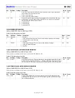
SCRATCH BUFFER REGISTER
Address: 0x4000501C, Reset: 0x0000, Name: COMSCR
Table 329. Bit Descriptions for COMSCR
Bits Bit
Name
Settings
Description
Reset Access
[15:8] Reserved
Reserved.
0x0 R
[7:0] SCR
Scratch. The scratch register is an 8-bit register used to store intermediate results. The
value contained in the scratch register does not affect UART functionality or performance.
Only eight bits of this register are implemented. Bits[15:8] are read only and always
return 0x00 when read. SCR is writable with any value from 0 to 255. A read returns the
last value written.
0x0 R/W
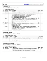
FIFO CONTROL REGISTER
Address: 0x40005020, Reset: 0x0000, Name: COMFCR
Table 330. Bit Descriptions for COMFCR
Bits Bit
Name
Settings
Description
Reset Access
[15:8] Reserved
Reserved.
0x0 R
[7:6]
RFTRIG
Receive FIFO Trigger Level.
0x0
R/W
00
1 byte to trigger receive interrupt.
01
4 byte to trigger receive interrupt.
10
8 byte to trigger receive interrupt.
11
14 byte to trigger receive interrupt.
[5:4] Reserved
Reserved.
0x0 R


