


UG-1262
Rev. B | Page 131 of 312
For example, when writing to the WGCON register directly through the die to die interface, Address 0x400C2014 is used. To write to the
same register using the sequencer, the address field must be 0b0000101 (Bits[8:2] of the address used by the external controller).
The data field is 24 bits wide and only allows writing to the MMR bits, Bits[23:0]. It is not possible to write to the full 32 bits of the MMRs via the
sequencer. However, Bits[31:24] are not used by any of the MMRs. Therefore, all assigned MMR bits can be written by the sequencer.
Timer Command
There are two timer commands in the sequencer, each with a separate hardware counter.
The wait command introduces wait states in the sequencer execution. When the programmed counter reaches 0, the execution resumes
by reading the next command from command memory.
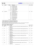
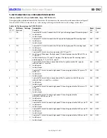
Figure 29 shows the format of the timer command, and Figure 30 shows the format of the wait command.
The timeout command starts a counter that operates independently of the sequencer flow. When the timer elapses, one of two interrupts is
generated: a sequencer timeout error interrupt (INTSEL17) or a sequencer timeout finished interrupt (INTSEL16). Both interrupts are
configured in the INTCSELx registers. The sequence timeout finished interrupt is asserted at the end of the timeout period. The sequence
timeout error interrupt is asserted if the sequencer does not reach the end of execution at the end of the timeout period. These interrupts
are cleared by writing to the corresponding bits in the INTCCLR register. The current value of the counter can be read by the host
controller at any time through the SEQTIMEOUT register.
The timeout counter is not reset when the sequencer execution is stopped as a result of a sequencer write command. However, the
counter resets if the host controller writes a 0 to the SEQEN bit in the SEQCON register. This reset applies to situations when the host
must abort the sequence.
The time unit for both timer commands is one ACLK period. For a clock frequency of 16 MHz, the timer resolution is 62.5 ns and the
maximum timeout is 67.1 sec. These values are still true when the SEQWRTMR bits in the SEQCON register are nonzero.
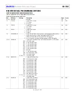
B31
BIT 31
COMMAND
BITS[30:24]
ADDR
BITS[23:0]
DATA
1
B30 B29 B28 B27 B26 B25 B24 B23 B22 B21 B20 B19 B18 B17 B16 B15 B14 B13 B12 B11 B10 B9 B8 B7 B6 B5 B4 B3 B2 B1 B0
166
75
-328
Figure 28. Sequencer Write Command
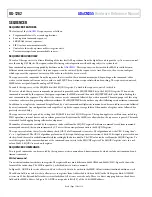
B31
BITS[31:30]
COMMAND
BITS[29:0]
TIME
0
1
B30 B29 B28 B27 B26 B25 B24 B23 B22 B21 B20 B19 B18 B17 B16 B15 B14 B13 B12 B11 B10 B9 B8 B7 B6 B5 B4 B3 B2 B1 B0
166
75
-329
Figure 29. Sequencer Timer Command
B31
BITS[31:30]
COMMAND
BITS[29:0]
TIME
0
0
B30 B29 B28 B27 B26 B25 B24 B23 B22 B21 B20 B19 B18 B17 B16 B15 B14 B13 B12 B11 B10 B9 B8 B7 B6 B5 B4 B3 B2 B1 B0
166
75-
330
Figure 30. Sequencer Wait Command
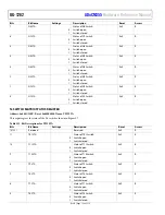
SEQUENCER OPERATION
Figure 31 shows the typical steps required to set up the sequencer to take measurements. When the device is booted up, take the following
steps to configure the sequencer, command memory, and data FIFO:
1.
Configure the command memory.
2.
Load the sequences into the SRAM.
3.
Set the Sequence 0 (SEQ0) to Sequence 3 (SEQ3) information sequences.
4.
Configure the data FIFO.
5.
Configure the sleep and wake-up timer.
6.
Configure the interrupts.
7.
Configure the sleep and wake-up method.


