


UG-1262
Rev. B | Page 103 of 312
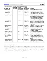
DE0RESCON, Bits[7:0] (DE0) and DE1RESCON, Bits[7:0] (DE1) Setting
R
LOAD03
and R
LOAD05
Value (Ω)
R
TIA2_03
and R
TIA2_05
Value
0x7A 30
40.07
kΩ
0x82 30
80.07
kΩ
0x8A 30
160.07
kΩ
0x1B 50
50
Ω
0x33 50
100
Ω
0x4B 50
190
Ω
0x5B 50
1.05
kΩ
0x63 50
5.05
kΩ
0x6B 50
10.05
kΩ
0x73 50
20.05
kΩ
0x7B 50
40.05
kΩ
0x83 50
80.05
kΩ
0x8B 50
160.05
kΩ
0x34 100
50
Ω
0x3C 100
100
Ω
0x54 100
200
Ω
0x5C 100
1
kΩ
0x64 100
5
kΩ
0x6C 100
10
kΩ
0x74 100
20
kΩ
0x7C 100
40
kΩ
0x84 100
80
kΩ
0x8C 100
160
kΩ
The high speed TIA common-mode voltage setting (positive input to the high speed TIA amplifier) is configurable via HSTIACON,
Bits[1:0]. The configuration options are as follows:
Internal 1.1 V reference source (same as ADCVBIAS_CAP pin voltage).
Sensor Channel 0 low power DAC output (VZERO0 pin). See Table 110 and Table 115 for details.
Sensor Channel 1 low power DAC output (VZERO1 pin). See Table 112 and Table 118 for details.
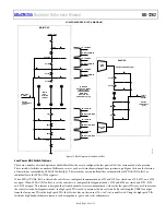
Figure 21 shows the high speed TIA connections to external pins and the programmable switch and resistor locations in this part of the
receive signal circuitry.
16
675
-021
AIN0
AIN1
AIN2
AIN3/BUF_VREF1V8
Tx SWITCHES
R
LOAD03
R
LOAD05
+
–
R
TIA2
HIGH SPEED
TRANSIMPEDANCE
AMPLIFIER
C
T7
T5
T3
T4
T2
T1
TIA_I
TIA_O
R
TIA2_05
R
TIA2_03
T9
T10
T11
TSWFULLCON
OR SWCON[15:12]
TSWFULLCON
OR SWCON TO
SET Tx SWITCHES
HSRTIACON[3:0]
HSRTIACON[12:5]
DE0RESCON[7:0]
DE1RESCON[7:0]
SW AND R
LOAD05
CONTROLLED BY
DE1RESCON[7:0]
SW AND R
LOAD03
CONTROLLED BY
DE0RESCON[7:0]
HSRTIACON[4]
DE0
DE1
HSTIACON[1:0]
SELECTS SOURCE
T6
T8
Figure 21. High Speed TIA Circuitry


