


UG-1262
Rev. B | Page 94 of 312
Bits Bit
Name
Settings
Description
Reset
Access
10101
120 kΩ. R
TIA
gain = 120 kΩ − (R
LOAD
− 100 Ω).
10110
128 kΩ. R
TIA
gain = 128 kΩ − (R
LOAD
− 100 Ω).
10111
160 kΩ. R
TIA
gain = 160 kΩ − (R
LOAD
− 100 Ω).
11000
196 kΩ. R
TIA
gain = 196 kΩ − (R
LOAD
− 100 Ω).
11001
256 kΩ. R
TIA
gain = 256 kΩ − (R
LOAD
− 100 Ω).
11010
512 kΩ. R
TIA
gain = 512 kΩ − (R
LOAD
− 100 Ω).
[4:3]
IBOOST
Current Boost Control.
0x0
R/W
00
Normal
mode.
01
Increase amplifier output stage current to quickly charge external capacitor load.
Intended for use with high current sensors, such as oxygen electrochemical sensor.
10
Double TIA and potentiostat amplifiers overall quiescent current. Increases amplifier
bandwidth. Useful for diagnostic tests.
11
Double TIA and potentiostat amplifiers overall quiescent current and increase output
stage current. Increases amplifier bandwidth and output current capability. Useful for
diagnostic tests with high current sensors like the oxygen electrochemical sensor.
2 HALFPWR
Half Power Mode Select. Control bit to reduce active power consumption of TIA and
potentiostat amplifiers for Sensor Channel 0.
0x0 R/W
0
Normal mode. Default value.
1
Reduce potentiostat amplifier and TIA current by half. Degrades performance.
1 PAPDEN
Potentiostat Amplifier Power Down. Low power Potentiostat Amplifier 0 power-down
control bit.
0x1 R/W
0
Power
up.
1
Power
down.
0
TIAPDEN
TIA Power Down. Low power TIA0 power-down control bit.
0x1
R/W
0
Power
up.
1
Power
down.
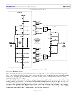
LOW POWER TIA SWITCH CONFIGURATION FOR CHANNEL 0 REGISTER
Address: 0x400C20E4, Reset: 0x00000000, Name: LPTIASW0
See Figure 16 for details on the switches mentioned in this register.
Table 110. Bit Descriptions for LPTIASW0
Bits Bit
Name Settings
Description
Reset
Access
[31:16] Reserved
Reserved.
0x0
R
15
RECAL
TIA SW15 Control. Active high.
0x0
R/W
0
Disconnect potentiostat amplifier for Channel 0 output from the RE0 pin.
1
Connect Potentiostat Amplifier 0 output to the RE0 pin.
14
VZEROSHARE
TIA SW14 Control. Active high.
0x0
R/W
0
Turn off switch. Default.
1
Short TIA0 input to TIA1 input and share the VZEROx pin.
13
TIABIASSEL
TIA SW13 Control. Active high.
0x0
R/W
0
Disconnect TIA bias voltage from the VZERO0 pin.
1
Connect TIA bias voltage to the VZERO0 pin.
12
PABIASSEL
TIA SW12 Control. Active high.
0x0
R/W
0
Disconnect potentiostat amplifier bias voltage from the VBIAS0 pin.
1
Connect potentiostat amplifier bias voltage to the VBIAS0 pin.
11
SW11
SW11 Switch Control Active High.
0x0
R/W
0
Open
switch.
1
Close
switch.
10
SW10
SW10 Switch Control Active High.
0x0
R/W
0
Open
switch.
1
Close
switch.


