


NUC126
Aug. 08, 2018
Page
317
of 943
Rev 1.03
NUC12
6 S
E
RI
E
S
T
E
CH
NI
CA
L R
E
F
E
RE
NCE
MA
NUA
L
uA for V
DD
is form 5.0 V to 2.5 V.
Port Pin
Port Pin
N
N
P
P
VDD
VDD
Port Latch Data
Port Latch Data
Input Data
Input Data
2 CPU
Clock Delay
P
P
P
P
Strong
Strong
Very
Weak
Very
Weak
Weak
Weak
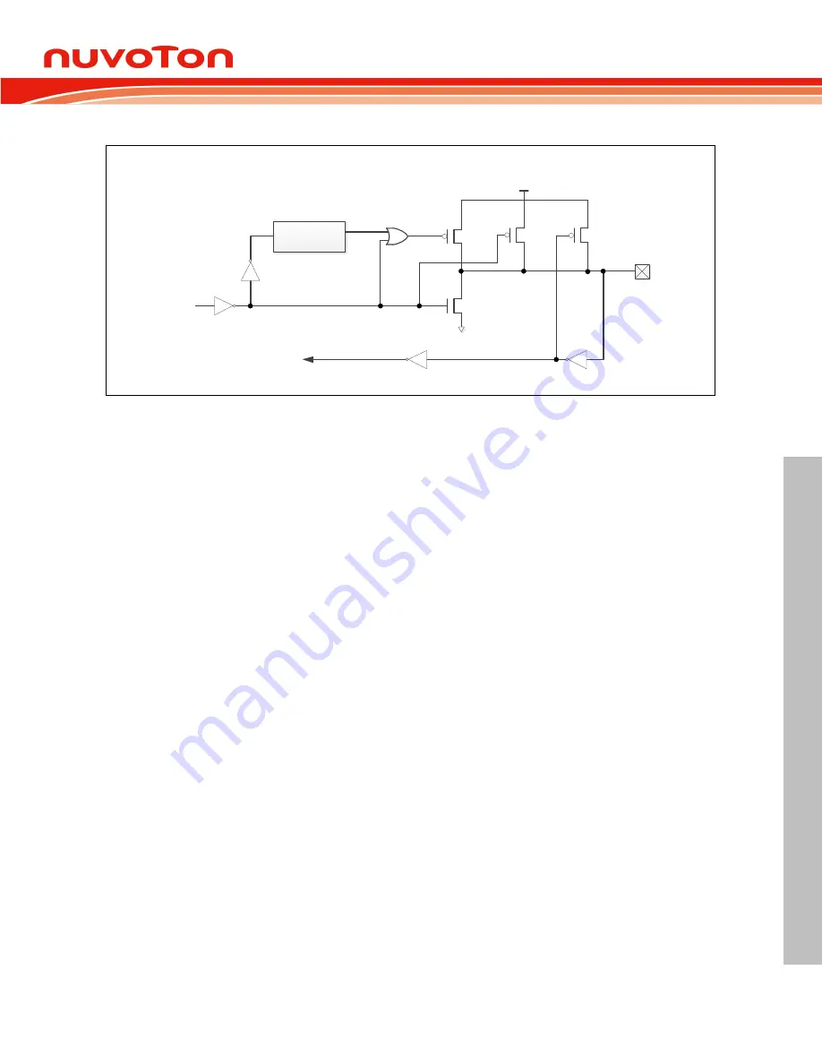
Figure 6.9-4 Quasi-Bidirectional I/O Mode
6.9.5.5
GPIO Interrupt and Wake-up Function
Each GPIO pin can be set as chip interrupt source by setting correlative RHIEN (Px_INTEN[n+16])/
FLIEN (Px_INTEN[n]) bit and TYPE (Px_INTTYPE[n]). There are five types of interrupt condition can
be selected: low level trigger, high level trigger, falling edge trigger, rising edge trigger and both rising
and falling edge trigger. For edge trigger condition, user can enable input signal de-bounce function to
prevent unexpected interrupt happened which caused by noise. The de-bounce clock source and
sampling cycle period can be set through DBCLKSRC (GPIO_DBCTL[4]) and DBCLKSEL
(GPIO_DBCTL[3:0]) register.
The GPIO can also be the chip wake-up source when chip enters Idle/Power-down mode. The setting
of wake-up trigger condition is the same as GPIO interrupt trigger.
6.9.5.6
GPIO Digital Input Path Disable Control
User can disable GPIO digital input path by setting DINOFF (Px_DINOFF[n]). When GPIO digital input
path is disabled, the digital input pin value PIN (Px_PIN[n]) is tied to low. By the way, the GPIO digital
input path is force disabled by hardware and DINOFF control is useless when I/O function configure as
ADC/ACMP/ext. XTL..