


MOTOROLA CMOS LOGIC DATA
6–509
MC14585B
ÎÎÎÎÎÎÎÎÎÎÎÎÎÎÎÎÎÎÎÎÎÎÎÎÎÎÎÎÎÎÎÎÎÎ
ÎÎÎÎÎÎÎÎÎÎÎÎÎÎÎÎÎÎÎÎÎÎÎÎÎÎÎÎÎÎÎÎÎÎ
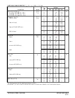
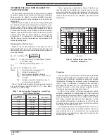
SWITCHING CHARACTERISTICS*
(CL = 50 pF, TA = 25
_
C)
Characteristic
Symbol
VDD
Min
Typ #
Max
Unit
Output Rise and Fall Time
tTLH, tTHL = (1.5 ns/pF) CL + 25 ns
tTLH, tTHL = (0.75 ns/pF) CL + 12.5 ns
tTLH, tTHL = (0.55 ns/pF) CL + 9.5 ns
tTLH,
tTHL
5.0
10
15
—
—
—
100
50
40
200
100
80
ns
Turn–On, Turn–Off Delay Time
tPLH, tPHL = (1.7 ns/pF) CL + 345 ns
tPLH, tPHL = (0.66 ns/pF) CL + 147 ns
tPLH, tPHL = (0.5 ns/pF) CL + 105 ns
tPLH,
tPHL
5.0
10
15
—
—
—
430
180
130
860
360
260
ns
* The formulas given are for the typical characteristics only at 25
_
C.
#Data labelled “Typ” is not to be used for design purposes but is intended as an indication of the IC’s potential performance.
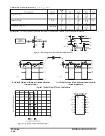
Figure 1. Dynamic Power Dissipation
Signal Waveforms
Figure 2. Dynamic Signal Waveforms
20 ns
20 ns
2f
1
VDD
VSS
VDD
VSS
VOH
VOL
VOH
VOL
VOH
VOL
(A < B)out
(A = B)out
(A > B)out
B3
A3
20 ns
20 ns
VDD
VSS
VOH
VOL
90%
50%
10%
tPLH
tPHL
tTLH
tTHL
90%
50%
10%
B0
(A = B)out
(A < B)out
Inputs (A>B) and (A=B) high, and inputs B3, A3, B2,
A2, B1, A1, A0, and (A<B) low.
Inputs (A>B) and (A=B) high, and inputs B2, A2, B1,
A1, B0, A0 and (A<B) low.
f in respect to a system clock.
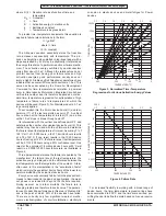
This device contains protection circuitry to guard against damage due to high static voltages or electric fields. However,
precautions must be taken to avoid applications of any voltage higher than maximum rated voltages to this high-impedance
circuit. For proper operation, Vin and Vout should be constrained to the range VSS
≤
(Vin or Vout)
≤
VDD.
Unused inputs must always be tied to an appropriate logic voltage level (e.g., either VSS or VDD). Unused outputs must
be left open.
Содержание CMOS Logic
Страница 1: ......
Страница 5: ...iv MOTOROLA CMOS LOGIC DATA ...
Страница 6: ...Master Index 1 ...
Страница 12: ...Product Selection Guide 2 ...
Страница 17: ...The Better Program 3 ...
Страница 20: ...B and UB Series Family Data 4 ...
Страница 25: ...CMOS Handling and Design Guidelines 5 ...
Страница 32: ...CMOS Handling and Design Guidelines 5 ...
Страница 39: ...Data Sheets 6 ...
Страница 69: ...MOTOROLA CMOS LOGIC DATA 6 31 MC14008B Figure 5 Logic Diagram Cin A1 B1 A2 B2 A3 B3 A4 B4 S1 S2 S3 S4 Cout ...
Страница 234: ...MOTOROLA CMOS LOGIC DATA MC14174B 6 196 FUNCTIONAL BLOCK DIAGRAM TIMING DIAGRAM ...
Страница 238: ...MOTOROLA CMOS LOGIC DATA MC14175B 6 200 FUNCTIONAL BLOCK DIAGRAM TIMING DIAGRAM ...
Страница 555: ...CMOS Reliability 7 ...
Страница 561: ...Equivalent Gate Count 8 ...
Страница 563: ...Packaging Information Including Surface Mounts 9 ...
Страница 571: ......