


MOTOROLA CMOS LOGIC DATA
6–385
MC14543B
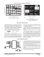
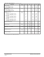
Figure 1. Typical Output Source
Characteristics
Figure 2. Typical Output Sink
Characteristics
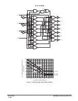
– 24
– 18
– 12
– 6.0
0
I OH
, SOURCE CURRENT
(mAdc)
(VOH – VDD), SOURCE DEVICE VOLTAGE (Vdc)
– 16
– 12
– 8.0
– 4.0
0
VDD = 5.0 Vdc
POHmax = 70 mWdc
VDD = 10 Vdc
VDD = 15 Vdc
VSS = 0 Vdc
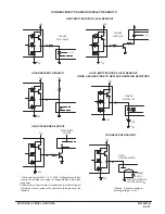
0
6.0
12
18
24
I OL
, SINK CURRENT
(mAdc)
(VOL – VSS), SINK DEVICE VOLTAGE (Vdc)
0
4.0
8.0
12
16
VDD = 15 Vdc
VDD = 10 Vdc
VDD = 5.0 Vdc
VSS = 0 Vdc
POLmax = 70 mWdc
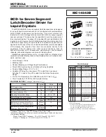
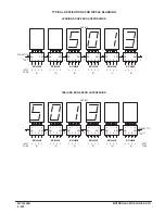
Figure 3. Dynamic Power Dissipation
Signal Waveforms
Inputs BI and Ph low, and Inputs D and LD high.
f in respect to a system clock.
Figure 4. Dynamic Signal Waveforms
(a) Inputs D, Ph, and BI low, and Inputs A, B, and LD high.
(b) Inputs D, Ph, and BI low, and Inputs A and B high.
(c) Data DCBA strobed into latches
20 ns
20 ns
VDD
VSS
VOH
VOL
10%
50%
90%
1
2f
50% DUTY CYCLE
A, B, AND C
ANY OUTPUT
All outputs connected to respective CL loads.
20 ns
20 ns
90%
10%
50%
tPHL
tPLH
90%
50%
10%
VDD
VSS
VOH
VOL
VDD
VSS
VDD
VSS
VOH
VOL
VDD
VSS
tTHL
tTLH
C
g
LD
C
g
LD
20 ns
90%
50%
10%
50%
50%
th
tsu
50%
tWH
Содержание CMOS Logic
Страница 1: ......
Страница 5: ...iv MOTOROLA CMOS LOGIC DATA ...
Страница 6: ...Master Index 1 ...
Страница 12: ...Product Selection Guide 2 ...
Страница 17: ...The Better Program 3 ...
Страница 20: ...B and UB Series Family Data 4 ...
Страница 25: ...CMOS Handling and Design Guidelines 5 ...
Страница 32: ...CMOS Handling and Design Guidelines 5 ...
Страница 39: ...Data Sheets 6 ...
Страница 69: ...MOTOROLA CMOS LOGIC DATA 6 31 MC14008B Figure 5 Logic Diagram Cin A1 B1 A2 B2 A3 B3 A4 B4 S1 S2 S3 S4 Cout ...
Страница 234: ...MOTOROLA CMOS LOGIC DATA MC14174B 6 196 FUNCTIONAL BLOCK DIAGRAM TIMING DIAGRAM ...
Страница 238: ...MOTOROLA CMOS LOGIC DATA MC14175B 6 200 FUNCTIONAL BLOCK DIAGRAM TIMING DIAGRAM ...
Страница 555: ...CMOS Reliability 7 ...
Страница 561: ...Equivalent Gate Count 8 ...
Страница 563: ...Packaging Information Including Surface Mounts 9 ...
Страница 571: ......