


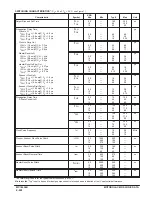


MOTOROLA CMOS LOGIC DATA
6–361
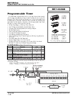
MC14536B
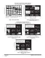
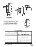
Figure 6. Power Dissipation Test
Circuit and Waveform
Figure 7. Switching Time Test Circuit and Waveforms
VDD
0.01
µ
F
CERAMIC
500
µ
F
ID
CL
CL
CL
VSS
PULSE
GENERATOR
SET
RESET
8–BYPASS
IN1
C INH
MONO IN
OSC INH
C
B
A
D
OUT 1
OUT
2
DECODE
OUT
20 ns
20 ns
90%
10%
50%
50%
DUTY CYCLE
PULSE
GENERATOR
SET
RESET
8–BYPASS
IN1
C INH
MONO IN
OSC INH
C
B
A
D
OUT 1
OUT
2
DECODE
OUT
CL
VSS
VDD
20 ns
20 ns
50%
IN1
tWL
tWH
50%
tPHL
90%
10%
tPLH
tTLH
tTHL
OUT
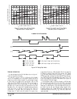
FUNCTIONAL TEST SEQUENCE
Test function (Figure 8) has been included for the reduc-
tion of test time required to exercise all 24 counter stages.
This test function divides the counter into three 8–stage
sections and 255 counts are loaded in each of the 8–stage
sections in parallel. All flip–flops are now at a “1”. The count-
er is now returned to the normal 24–stages in series configu-
ration. One more pulse is entered into In1 which will cause
the counter to ripple from an all “1” state to an all “0” state.
Figure 8. Functional Test Circuit
VDD
VSS
PULSE
GENERATOR
SET
RESET
8–BYPASS
IN1
C INH
MONO IN
OSC INH
C
B
A
D
OUT 1
OUT
2
DECODE
OUT
FUNCTIONAL TEST SEQUENCE
Inputs
Outputs
Comments
In1
Set
Reset
8–Bypass
Decade Out
Q1 thru Q24
All 24 stages are in Reset mode.
1
0
1
1
0
g
1
1
1
1
0
Counter is in three 8 stage sections in parallel mode.
0
1
1
1
0
First “1” to “0” transition of clock.
1
0
—
—
—
1
1
1
255 “1” to “0” transitions are clocked in the counter.
0
1
1
1
1
The 255 “1” to “0” transition.
0
0
0
0
1
Counter converted back to 24 stages in series mode.
Set and Reset must be connected together and simultaneously
go from “1” to “0”.
1
0
0
0
1
In1 Switches to a “1”.
0
0
0
0
0
Counter Ripples from an all “1” state to an all “0” state.
Содержание CMOS Logic
Страница 1: ......
Страница 5: ...iv MOTOROLA CMOS LOGIC DATA ...
Страница 6: ...Master Index 1 ...
Страница 12: ...Product Selection Guide 2 ...
Страница 17: ...The Better Program 3 ...
Страница 20: ...B and UB Series Family Data 4 ...
Страница 25: ...CMOS Handling and Design Guidelines 5 ...
Страница 32: ...CMOS Handling and Design Guidelines 5 ...
Страница 39: ...Data Sheets 6 ...
Страница 69: ...MOTOROLA CMOS LOGIC DATA 6 31 MC14008B Figure 5 Logic Diagram Cin A1 B1 A2 B2 A3 B3 A4 B4 S1 S2 S3 S4 Cout ...
Страница 234: ...MOTOROLA CMOS LOGIC DATA MC14174B 6 196 FUNCTIONAL BLOCK DIAGRAM TIMING DIAGRAM ...
Страница 238: ...MOTOROLA CMOS LOGIC DATA MC14175B 6 200 FUNCTIONAL BLOCK DIAGRAM TIMING DIAGRAM ...
Страница 555: ...CMOS Reliability 7 ...
Страница 561: ...Equivalent Gate Count 8 ...
Страница 563: ...Packaging Information Including Surface Mounts 9 ...
Страница 571: ......