


MOTOROLA CMOS LOGIC DATA
6–129
MC14049UB
Hex Buffers
The MC14049UB hex inverter/buffer is constructed with MOS P–channel
and N–channel enhancement mode devices in a single monolithic structure.
This complementary MOS device finds primary use where low power
dissipation and/or high noise immunity is desired. This device provides
logic–level conversion using only one supply voltage, VDD. The input–signal
high level (VIH) can exceed the VDD supply voltage for logic–level
conversions. Two TTL/DTL Loads can be driven when the device is used as
CMOS–to–TTL/DTL converters (VDD = 5.0 V, VOL
v
0.4 V, IOL
≥
3.2 mA).
Note that pins 13 and 16 are not connected internally on this device;
consequently connections to these terminals will not affect circuit operation.
•
High Source and Sink Currents
•
High–to–Low Level Converter
•
Supply Voltage Range = 3.0 V to 18 V
•
Meets JEDEC UB Specifications
•
VIN can exceed VDD
•
Improved ESD Protection on All Inputs
ÎÎÎÎÎÎÎÎÎÎÎÎÎÎÎÎÎÎÎÎÎ
ÎÎÎÎÎÎÎÎÎÎÎÎÎÎÎÎÎÎÎÎÎ
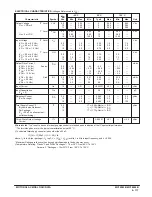
MAXIMUM RATINGS*
(Voltages Referenced to VSS)
ÎÎÎÎÎÎÎÎÎÎÎÎ
ÎÎÎÎÎÎÎÎÎÎÎÎ
Rating
ÎÎÎ
ÎÎÎ
Symbol
ÎÎÎÎÎÎ
ÎÎÎÎÎÎ
Value
ÎÎÎ
ÎÎÎ
Unit
ÎÎÎÎÎÎÎÎÎÎÎÎ
ÎÎÎÎÎÎÎÎÎÎÎÎ
DC Supply Voltage
ÎÎÎ
ÎÎÎ
VDD
ÎÎÎÎÎÎ
ÎÎÎÎÎÎ
– 0.5 to + 18
ÎÎÎ
ÎÎÎ
V
ÎÎÎÎÎÎÎÎÎÎÎÎ
ÎÎÎÎÎÎÎÎÎÎÎÎ
Input Voltage (DC or Transient)
ÎÎÎ
ÎÎÎ
Vin
ÎÎÎÎÎÎ
ÎÎÎÎÎÎ
– 0.5 to + 18
ÎÎÎ
ÎÎÎ
V
ÎÎÎÎÎÎÎÎÎÎÎÎ
ÎÎÎÎÎÎÎÎÎÎÎÎ
Output Voltage (DC or Transient)
ÎÎÎ
ÎÎÎ
Vout
ÎÎÎÎÎÎ
ÎÎÎÎÎÎ
– 0.5 to VDD + 0.5
ÎÎÎ
ÎÎÎ
V
ÎÎÎÎÎÎÎÎÎÎÎÎ
ÎÎÎÎÎÎÎÎÎÎÎÎ
Input Current (DC or Transient), per Pin
ÎÎÎ
ÎÎÎ
Iin
ÎÎÎÎÎÎ
ÎÎÎÎÎÎ
±
10
ÎÎÎ
ÎÎÎ
mA
ÎÎÎÎÎÎÎÎÎÎÎÎ
ÎÎÎÎÎÎÎÎÎÎÎÎ
Output Current (DC or Transient), per Pin
ÎÎÎ
ÎÎÎ
Iout
ÎÎÎÎÎÎ
ÎÎÎÎÎÎ
+ 45
ÎÎÎ
ÎÎÎ
mA
ÎÎÎÎÎÎÎÎÎÎÎÎ
Î
ÎÎÎÎÎÎÎÎÎÎ
Î
Î
ÎÎÎÎÎÎÎÎÎÎ
Î
ÎÎÎÎÎÎÎÎÎÎÎÎ
Power Dissipation, per Package†
Plastic/Ceramic
SOIC
ÎÎÎ
Î
Î
Î
Î
Î
Î
ÎÎÎ
PD
ÎÎÎÎÎÎ
Î
ÎÎÎÎ
Î
Î
ÎÎÎÎ
Î
ÎÎÎÎÎÎ
825
740
ÎÎÎ
Î
Î
Î
Î
Î
Î
ÎÎÎ
mW
ÎÎÎÎÎÎÎÎÎÎÎÎ
ÎÎÎÎÎÎÎÎÎÎÎÎ
Storage Temperature
ÎÎÎ
ÎÎÎ
Tstg
ÎÎÎÎÎÎ
ÎÎÎÎÎÎ
– 65 to + 150
ÎÎÎ
ÎÎÎ
_
C
ÎÎÎÎÎÎÎÎÎÎÎÎ
ÎÎÎÎÎÎÎÎÎÎÎÎ
Lead Temperature (8–Second Soldering)
ÎÎÎ
ÎÎÎ
TL
ÎÎÎÎÎÎ
ÎÎÎÎÎÎ
260
ÎÎÎ
ÎÎÎ
_
C
* Maximum Ratings are those values beyond which damage to the device may occur.
†Temperature Derating: All Packages: See Figure 4.
CIRCUIT SCHEMATIC
(1/6 OF CIRCUIT SHOWN)
VDD
VSS
MC14049UB
MOTOROLA
SEMICONDUCTOR TECHNICAL DATA
MC14049UB
L SUFFIX
CERAMIC
CASE 620
ORDERING INFORMATION
MC14XXXBCP
Plastic
MC14XXXBCL
Ceramic
MC14XXXBD
SOIC
TA = – 55
°
to 125
°
C for all packages.
P SUFFIX
PLASTIC
CASE 648
D SUFFIX
SOIC
CASE 751B
LOGIC DIAGRAM
MC14049UB
14
15
11
9
7
5
3
12
10
6
4
2
NC = PIN 13, 16
VSS = PIN 8
VDD = PIN 1
Содержание CMOS Logic
Страница 1: ......
Страница 5: ...iv MOTOROLA CMOS LOGIC DATA ...
Страница 6: ...Master Index 1 ...
Страница 12: ...Product Selection Guide 2 ...
Страница 17: ...The Better Program 3 ...
Страница 20: ...B and UB Series Family Data 4 ...
Страница 25: ...CMOS Handling and Design Guidelines 5 ...
Страница 32: ...CMOS Handling and Design Guidelines 5 ...
Страница 39: ...Data Sheets 6 ...
Страница 69: ...MOTOROLA CMOS LOGIC DATA 6 31 MC14008B Figure 5 Logic Diagram Cin A1 B1 A2 B2 A3 B3 A4 B4 S1 S2 S3 S4 Cout ...
Страница 234: ...MOTOROLA CMOS LOGIC DATA MC14174B 6 196 FUNCTIONAL BLOCK DIAGRAM TIMING DIAGRAM ...
Страница 238: ...MOTOROLA CMOS LOGIC DATA MC14175B 6 200 FUNCTIONAL BLOCK DIAGRAM TIMING DIAGRAM ...
Страница 555: ...CMOS Reliability 7 ...
Страница 561: ...Equivalent Gate Count 8 ...
Страница 563: ...Packaging Information Including Surface Mounts 9 ...
Страница 571: ......