


MOTOROLA CMOS LOGIC DATA
MC14583B
6–498
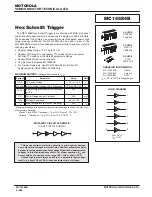
Dual Schmitt Trigger
The MC14583B is a dual Schmitt trigger constructed with complementary
P–channel and N–channel MOS devices on a monolithic silicon substrate.
Each Schmitt trigger is functionally independent except for a common
3–state input and an internally–connected Exclusive OR output for use in
line receiver applications. Trigger levels are adjustable through the positive,
negative, and common terminals with the use of external resistors.
Applications include the speed–up of a slow waveform edge in interface
receivers, level detectors, etc.
•
Diode Protection on All Inputs
•
Supply Voltage Range = 3.0 Vdc to 18 Vdc
•
Single Supply Operation
•
Capable of Driving Two Low–power TTL Loads or One Low–power
Schottky TTL Load Over the Rated Temperature Range
•
Resistor Adjustable Trigger Levels
ÎÎÎÎÎÎÎÎÎÎÎÎÎÎÎÎÎÎÎÎÎ
ÎÎÎÎÎÎÎÎÎÎÎÎÎÎÎÎÎÎÎÎÎ
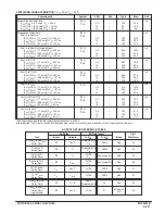
MAXIMUM RATINGS*
(Voltages Referenced to VSS)
Symbol
Parameter
Value
Unit
VDD
DC Supply Voltage
– 0.5 to + 18.0
V
Vin, Vout Input or Output Voltage (DC or Transient)
– 0.5 to VDD + 0.5
V
Iin, Iout
Input or Output Current (DC or Transient),
per Pin
±
10
mA
PD
Power Dissipation, per Package†
500
mW
Tstg
Storage Temperature
– 65 to + 150
_
C
TL
Lead Temperature (8–Second Soldering)
260
_
C
* Maximum Ratings are those values beyond which damage to the device may occur.
†Temperature Derating:
Plastic “P and D/DW” Packages: – 7.0 mW/
_
C From 65
_
C To 125
_
C
Ceramic “L” Packages: – 12 mW/
_
C From 100
_
C To 125
_
C
LOGIC DIAGRAM
POSITIVE A
6 5
NEGATIVE A
7 COMMON A
Bout
9
Ain
12
Bout
10
EXCLUSIVE OR
14
Aout
11
Aout
4
13
15
Bin
POSITIVE B2
2 3
NEGATIVE B
1 COMMON B
3–STATE
OUTPUT DISABLE
VDD = PIN 16
VSS = PIN 8
MOTOROLA
SEMICONDUCTOR TECHNICAL DATA
MC14583B
L SUFFIX
CERAMIC
CASE 620
ORDERING INFORMATION
MC14XXXBCP
Plastic
MC14XXXBCL
Ceramic
MC14XXXBD
SOIC
TA = – 55
°
to 125
°
C for all packages.
P SUFFIX
PLASTIC
CASE 648
D SUFFIX
SOIC
CASE 751B
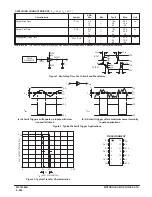
BLOCK DIAGRAM
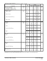
TRUTH TABLE
Inputs
Outputs
A
B
Dis Aout Aout Bout Bout
ę
0
0
0
0
Z
0
Z
0
0
0
1
0
1
0
1
0
0
1
0
0
Z
1
Z
1
0
1
1
0
1
1
0
1
1
0
0
1
Z
0
Z
1
1
0
1
1
0
0
1
1
1
1
0
1
Z
1
Z
0
1
1
1
1
0
1
0
0
Z = High impedance at output
VDD = PIN 16
VSS = PIN 8
9
13
15
12
10
14
11
4
APos ANeg ACom
BPos BNeg BCom
Ain
Bin
Dis
Bout
Bout
Aout
Aout
6
5
7
2
3
1
Содержание CMOS Logic
Страница 1: ......
Страница 5: ...iv MOTOROLA CMOS LOGIC DATA ...
Страница 6: ...Master Index 1 ...
Страница 12: ...Product Selection Guide 2 ...
Страница 17: ...The Better Program 3 ...
Страница 20: ...B and UB Series Family Data 4 ...
Страница 25: ...CMOS Handling and Design Guidelines 5 ...
Страница 32: ...CMOS Handling and Design Guidelines 5 ...
Страница 39: ...Data Sheets 6 ...
Страница 69: ...MOTOROLA CMOS LOGIC DATA 6 31 MC14008B Figure 5 Logic Diagram Cin A1 B1 A2 B2 A3 B3 A4 B4 S1 S2 S3 S4 Cout ...
Страница 234: ...MOTOROLA CMOS LOGIC DATA MC14174B 6 196 FUNCTIONAL BLOCK DIAGRAM TIMING DIAGRAM ...
Страница 238: ...MOTOROLA CMOS LOGIC DATA MC14175B 6 200 FUNCTIONAL BLOCK DIAGRAM TIMING DIAGRAM ...
Страница 555: ...CMOS Reliability 7 ...
Страница 561: ...Equivalent Gate Count 8 ...
Страница 563: ...Packaging Information Including Surface Mounts 9 ...
Страница 571: ......