


MOTOROLA CMOS LOGIC DATA
MC14536B
6–364
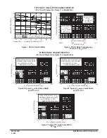
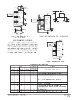
Figure 11. Time Interval Configuration Using On–Chip RC Oscillator and
Reset Input to Initiate Time Interval
(Divide–by–2 Configured)
NOTE: This circuit is designed to use the on–chip oscillation function. The oscillator frequency is deter-
mined by the external R and C components. When power is first applied to the device, Decode Out
initializes to a high state. Because this output is tied directly to the Osc–Inh input, the oscillator is
disabled. This puts the device in a low–current standby condition. The rising edge of the Reset pulse
will cause the output to go low. This in turn causes Osc–Inh to go low. However, while Reset is high,
the oscillator is still disabled (i.e.: standy condition). After Reset goes low, the output remains low
for 2n/2 of the oscillator’s period. After the part times out, the output again goes high.
PULSE
GEN.
8–BYPASS
A
B
C
D
RESET
SET
CLOCK INH
MONO–IN
CLOCK INH
IN1
VSS
DECODE OUT
OUT 2
OUT 1
8
16
+V
6
9
10
11
12
2
14
15
1
7
3
13
5
4
VDD
RS
RTC
C
OUT 2
OUT 1
RESET
POWER UP
Rs
F
R
C
DECODE OUT
tw
≥
Rtc
= Hz
= Ohms
= FARADS
fosc
^
1
2.3 Rtc C
Содержание CMOS Logic
Страница 1: ......
Страница 5: ...iv MOTOROLA CMOS LOGIC DATA ...
Страница 6: ...Master Index 1 ...
Страница 12: ...Product Selection Guide 2 ...
Страница 17: ...The Better Program 3 ...
Страница 20: ...B and UB Series Family Data 4 ...
Страница 25: ...CMOS Handling and Design Guidelines 5 ...
Страница 32: ...CMOS Handling and Design Guidelines 5 ...
Страница 39: ...Data Sheets 6 ...
Страница 69: ...MOTOROLA CMOS LOGIC DATA 6 31 MC14008B Figure 5 Logic Diagram Cin A1 B1 A2 B2 A3 B3 A4 B4 S1 S2 S3 S4 Cout ...
Страница 234: ...MOTOROLA CMOS LOGIC DATA MC14174B 6 196 FUNCTIONAL BLOCK DIAGRAM TIMING DIAGRAM ...
Страница 238: ...MOTOROLA CMOS LOGIC DATA MC14175B 6 200 FUNCTIONAL BLOCK DIAGRAM TIMING DIAGRAM ...
Страница 555: ...CMOS Reliability 7 ...
Страница 561: ...Equivalent Gate Count 8 ...
Страница 563: ...Packaging Information Including Surface Mounts 9 ...
Страница 571: ......