


MOTOROLA CMOS LOGIC DATA
MC14528B
6–322
ÎÎÎÎÎÎÎÎÎÎÎÎÎÎÎÎÎÎÎÎÎÎÎÎÎÎÎÎÎÎÎÎÎÎ
ÎÎÎÎÎÎÎÎÎÎÎÎÎÎÎÎÎÎÎÎÎÎÎÎÎÎÎÎÎÎÎÎÎÎ
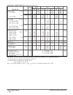
ELECTRICAL CHARACTERISTICS
(Voltages Referenced to VSS)
VDD
– 55
_
C
25
_
C
125
_
C
Characteristic
Symbol
Vdc
Min
Max
Min
Typ #
Max
Min
Max
Unit
Output Voltage
“0” Level
Vin = VDD or 0
VOL
5.0
10
15
—
—
—
0.05
0.05
0.05
—
—
—
0
0
0
0.05
0.05
0.05
—
—
—
0.05
0.05
0.05
Vdc
“1” Level
Vin = 0 or VDD
VOH
5.0
10
15
4.95
9.95
14.95
—
—
—
4.95
9.95
14.95
5.0
10
15
—
—
—
4.95
9.95
14.95
—
—
—
Vdc
Input Voltage
“0” Level
(VO = 4.5 or 0.5 Vdc)
(VO = 9.0 or 1.0 Vdc)
(VO = 13.5 or 1.5 Vdc)
VIL
5.0
10
15
—
—
—
1.5
3.0
4.0
—
—
—
2.25
4.50
6.75
1.5
3.0
4.0
—
—
—
1.5
3.0
4.0
Vdc
“1” Level
(VO = 0.5 or 4.5 Vdc)
(VO = 1.0 or 9.0 Vdc)
(VO = 1.5 or 13.5 Vdc)
VIH
5.0
10
15
3.5
7.0
11
—
—
—
3.5
7.0
11
2.75
5.50
8.25
—
—
—
3.5
7.0
11
—
—
—
Vdc
Output Drive Current
(VOH = 2.5 Vdc)
Source
(VOH = 4.6 Vdc)
(VOH = 9.5 Vdc)
(VOH = 13.5 Vdc)
IOH
5.0
5.0
10
15
– 1.2
– 0.64
– 1.6
– 4.2
—
—
—
—
– 1.0
– 0.51
– 1.3
– 3.4
– 1.7
– 0.88
– 2.25
– 8.8
—
—
—
—
– 0.7
– 0.36
– 0.9
– 2.4
—
—
—
—
mAdc
(VOL = 0.4 Vdc)
Sink
(VOL = 0.5 Vdc)
(VOL = 1.5 Vdc)
IOL
5.0
10
15
0.64
1.6
4.2
—
—
—
0.51
1.3
3.4
0.88
2.25
8.8
—
—
—
0.36
0.9
2.4
—
—
—
mAdc
Input Current
Iin
15
—
±
0.1
—
±
0.00001
±
0.1
—
±
1.0
µ
Adc
Input Capacitance
(Vin = 0)
Cin
—
—
—
—
5.0
7.5
—
—
pF
Quiescent Current
(Per Package)
IDD
5.0
10
15
—
—
—
5.0
10
20
—
—
—
0.005
0.010
0.015
5.0
10
20
—
—
—
150
300
600
µ
Adc
**Total Supply Current at an
external load Capacitance (CL)
and at external timing
capacitance (CX), use the
formula —
IT
—
IT(CL, CX) = [(CL + 0.36CX)VDDf + 2x10⁻⁸
RXCX(VDD–2)2f] x 10–3
where: IT in
µ
A (per circuit), CL and CX in pF, RX in megohms,
VDD in Vdc, f in kHz is input frequency.
µ
Adc
#Data labelled “Typ” is not to be used for design purposes but is intended as an indication of the IC’s potential performance.
** The formulas given are for the typical characteristics only at 25
_
C.
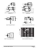
This device contains protection circuitry to guard against damage
due to high static voltages or electric fields. However, precautions must
be taken to avoid applications of any voltage higher than maximum rated
voltages to this high-impedance circuit. For proper operation, Vin and
Vout should be constrained to the range VSS
≤
(Vin or Vout)
≤
VDD.
Unused inputs must always be tied to an appropriate logic voltage
level (e.g., either VSS or VDD). Unused outputs must be left open.
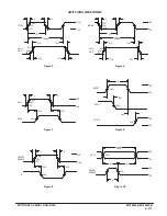
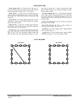
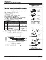
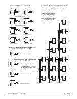
PIN ASSIGNMENT
13
14
15
16
9
10
11
12
5
4
3
2
1
8
7
6
A2
RESET 2
CX2/RX2
VSS
VDD
Q2
Q2
B2
A1
RESET 1
CX1/RX1
VSS
VSS
Q1
Q1
B1
Содержание CMOS Logic
Страница 1: ......
Страница 5: ...iv MOTOROLA CMOS LOGIC DATA ...
Страница 6: ...Master Index 1 ...
Страница 12: ...Product Selection Guide 2 ...
Страница 17: ...The Better Program 3 ...
Страница 20: ...B and UB Series Family Data 4 ...
Страница 25: ...CMOS Handling and Design Guidelines 5 ...
Страница 32: ...CMOS Handling and Design Guidelines 5 ...
Страница 39: ...Data Sheets 6 ...
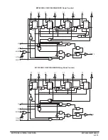
Страница 69: ...MOTOROLA CMOS LOGIC DATA 6 31 MC14008B Figure 5 Logic Diagram Cin A1 B1 A2 B2 A3 B3 A4 B4 S1 S2 S3 S4 Cout ...
Страница 234: ...MOTOROLA CMOS LOGIC DATA MC14174B 6 196 FUNCTIONAL BLOCK DIAGRAM TIMING DIAGRAM ...
Страница 238: ...MOTOROLA CMOS LOGIC DATA MC14175B 6 200 FUNCTIONAL BLOCK DIAGRAM TIMING DIAGRAM ...
Страница 555: ...CMOS Reliability 7 ...
Страница 561: ...Equivalent Gate Count 8 ...
Страница 563: ...Packaging Information Including Surface Mounts 9 ...
Страница 571: ......