


MOTOROLA CMOS LOGIC DATA
MC14536B
6–356
ÎÎÎÎÎÎÎÎÎÎÎÎÎÎÎÎÎÎÎÎÎÎÎÎÎÎÎÎÎÎÎÎÎÎ
ÎÎÎÎÎÎÎÎÎÎÎÎÎÎÎÎÎÎÎÎÎÎÎÎÎÎÎÎÎÎÎÎÎÎ
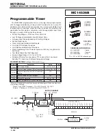
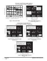
SWITCHING CHARACTERISTICS*
(CL = 50 pF, TA = 25
_
C)
Characteristic
Symbol
VDD
Min
Typ #
Max
Unit
Output Rise and Fall Time (Pin 13)
tTLH, tTHL = (1.5 ns/pF) CL + 25 ns
tTLH, tTHL = (0.75 ns/pF) CL + 12.5 ns
tTLH, tTHL = (0.55 ns/pF) CL + 9.5 ns
tTLH,
tTHL
5.0
10
15
—
—
—
100
50
40
200
100
80
ns
Propagation Delay Time
Clock to Q1, 8–Bypass (Pin 6) High
tPLH, tPHL = (1.7 ns/pF) CL + 1715 ns
tPLH, tPHL = (0.66 ns/pF) CL + 617 ns
tPLH, tPHL = (0.5 ns/pF) CL + 425 ns
tPLH,
tPHL
5.0
10
15
—
—
—
1800
650
450
3600
1300
1000
ns
Clock to Q1, 8–Bypass (Pin 6) Low
tPLH, tPHL = (1.7 ns/pF) CL + 3715 ns
tPLH, tPHL = (0.66 ns/pF) CL + 1467 ns
tPLH, tPHL = (0.5 ns/pF) CL + 1075 ns
tPLH,
tPHL
5.0
10
15
—
—
—
3.8
1.5
1.1
7.6
3.0
2.3
µ
s
Clock to Q16
tPHL, tPLH = (1.7 ns/pF) CL + 6915 ns
tPHL, tPLH = (0.66 ns/pF) CL + 2967 ns
tPHL, tPLH = (0.5 ns/pF) CL + 2175 ns
tPLH,
tPHL
5.0
10
15
—
—
—
7.0
3.0
2.2
14
6.0
4.5
µ
s
Reset to Qn
tPHL = (1.7 ns/pF) CL + 1415 ns
tPHL = (0.66 ns/pF) CL + 567 ns
tPHL = (0.5 ns/pF) CL + 425 ns
tPHL
5.0
10
15
—
—
—
1500
600
450
3000
1200
900
ns
Clock Pulse Width
tWH
5.0
10
15
600
200
170
300
100
85
—
—
—
ns
Clock Pulse Frequency
(50% Duty Cycle)
fcl
5.0
10
15
—
—
—
1.2
3.0
5.0
0.4
1.5
2.0
MHz
Clock Rise and Fall Time
tTLH,
tTHL
5.0
10
15
No Limit
—
Reset Pulse Width
tWH
5.0
10
15
1000
400
300
500
200
150
—
—
—
ns
* The formulas given are for the typical characteristics only at 25
_
C.
#Data labelled “Typ” is not to be used for design purposes but is intended as an indication of the IC’s potential performance.
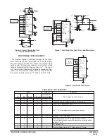
This device contains protection circuitry to guard against damage
due to high static voltages or electric fields. However, precautions must
be taken to avoid applications of any voltage higher than maximum rated
voltages to this high-impedance circuit. For proper operation, Vin and
Vout should be constrained to the range VSS
≤
(Vin or Vout)
≤
VDD.
Unused inputs must always be tied to an appropriate logic voltage
level (e.g., either VSS or VDD). Unused outputs must be left open.
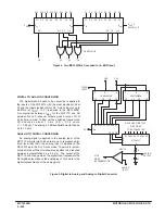
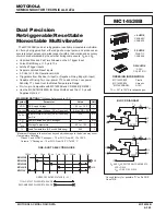
PIN ASSIGNMENT
13
14
15
16
9
10
11
12
5
4
3
2
1
8
7
6
D
DECODE
OSC INH
MONO IN
VDD
A
B
C
OUT 1
IN 1
RESET
SET
VSS
CLOCK INH
8–BYPASS
OUT 2
Содержание CMOS Logic
Страница 1: ......
Страница 5: ...iv MOTOROLA CMOS LOGIC DATA ...
Страница 6: ...Master Index 1 ...
Страница 12: ...Product Selection Guide 2 ...
Страница 17: ...The Better Program 3 ...
Страница 20: ...B and UB Series Family Data 4 ...
Страница 25: ...CMOS Handling and Design Guidelines 5 ...
Страница 32: ...CMOS Handling and Design Guidelines 5 ...
Страница 39: ...Data Sheets 6 ...
Страница 69: ...MOTOROLA CMOS LOGIC DATA 6 31 MC14008B Figure 5 Logic Diagram Cin A1 B1 A2 B2 A3 B3 A4 B4 S1 S2 S3 S4 Cout ...
Страница 234: ...MOTOROLA CMOS LOGIC DATA MC14174B 6 196 FUNCTIONAL BLOCK DIAGRAM TIMING DIAGRAM ...
Страница 238: ...MOTOROLA CMOS LOGIC DATA MC14175B 6 200 FUNCTIONAL BLOCK DIAGRAM TIMING DIAGRAM ...
Страница 555: ...CMOS Reliability 7 ...
Страница 561: ...Equivalent Gate Count 8 ...
Страница 563: ...Packaging Information Including Surface Mounts 9 ...
Страница 571: ......