


MOTOROLA CMOS LOGIC DATA
6–103
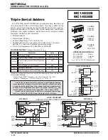
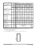
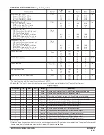
MC14034B
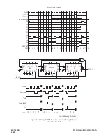
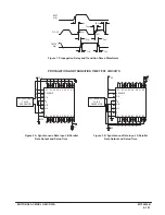
Figure 6. Shift Right/Shift Left with Parallel Inputs
A “High” (“Low”) on the Shift Left/Shift Right input allows serial data on the Shift Left Input (Shift Right Input) to enter the register
on the positive transition of the lock signal. A “high” on the “A” Enable Input disables the “A” parallel data lines on Reg. 1 and 2
and enables the “A” data lines on registers 3 and 4 and allows parallel data into registers 1 and 2. Other logic schemes may be
used in place of registers 3 and 4 for parallel loading.
When parallel inputs are not used, Reg. 3 and 4 and associated logic are not required.
*Shift left input must be disabled during parallel entry.
A ENABLE
SHIFT LEFT/
SHIFT RIGHT
SHIFT RIGHT
INPUT
CLOCK
A/S PARALLEL
ENTRY
REGISTER 1
MC14034B
SHIFT LEFT OUTPUT
AE
P/S
DS
A/B
A/S
CB1
B8
A1
A8
AE
P/S
DS
A/B
A/S
C
A1
A8
B1
B8
AE
P/S
SHIFT RIGHT
OUTPUT
REGISTER 2
MC14034B
SHIFT LEFT
INPUT*
A/S
COCK
AE
VDD
VDD
AE
P/S
DS
A/B
A/S
CB1
B8
REGISTER 3
MC14034B
REGISTER 4
MC14034B
A1
A8
AE
P/S
DS
A/B
A/S
C B1
B8
A1
A8
Содержание CMOS Logic
Страница 1: ......
Страница 5: ...iv MOTOROLA CMOS LOGIC DATA ...
Страница 6: ...Master Index 1 ...
Страница 12: ...Product Selection Guide 2 ...
Страница 17: ...The Better Program 3 ...
Страница 20: ...B and UB Series Family Data 4 ...
Страница 25: ...CMOS Handling and Design Guidelines 5 ...
Страница 32: ...CMOS Handling and Design Guidelines 5 ...
Страница 39: ...Data Sheets 6 ...
Страница 69: ...MOTOROLA CMOS LOGIC DATA 6 31 MC14008B Figure 5 Logic Diagram Cin A1 B1 A2 B2 A3 B3 A4 B4 S1 S2 S3 S4 Cout ...
Страница 234: ...MOTOROLA CMOS LOGIC DATA MC14174B 6 196 FUNCTIONAL BLOCK DIAGRAM TIMING DIAGRAM ...
Страница 238: ...MOTOROLA CMOS LOGIC DATA MC14175B 6 200 FUNCTIONAL BLOCK DIAGRAM TIMING DIAGRAM ...
Страница 555: ...CMOS Reliability 7 ...
Страница 561: ...Equivalent Gate Count 8 ...
Страница 563: ...Packaging Information Including Surface Mounts 9 ...
Страница 571: ......