


MOTOROLA CMOS LOGIC DATA
MC14094B
6–170
8-Stage Shift/Store Register
with Three-State Outputs
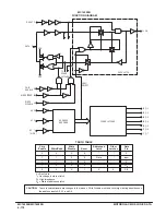
The MC14094B combines an 8–stage shift register with a data latch for
each stage and a three–state output from each latch.
Data is shifted on the positive clock transition and is shifted from the
seventh stage to two serial outputs. The QS output data is for use in
high–speed cascaded systems. The Q
′
S output data is shifted on the
following negative clock transition for use in low–speed cascaded systems.
Data from each stage of the shift register is latched on the negative
transition of the strobe input. Data propagates through the latch while strobe
is high.
Outputs of the eight data latches are controlled by three–state buffers
which are placed in the high–impedance state by a logic Low on Output
Enable.
•
Three–State Outputs
•
Capable of Driving Two Low–Power TTL Loads or One Low–Power
Schottky TTL Load Over the Rated Temperature Range
•
Input Diode Protection
•
Data Latch
•
Dual Outputs for Data Out on Both Positive and Negative Clock
Transitions
•
Useful for Serial–to–Parallel Data Conversion
•
Pin–for–Pin Compatible with CD4094B
ÎÎÎÎÎÎÎÎÎÎÎÎÎÎÎÎÎÎÎÎÎ
ÎÎÎÎÎÎÎÎÎÎÎÎÎÎÎÎÎÎÎÎÎ
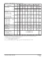
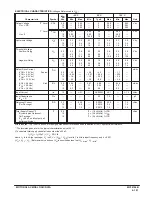
MAXIMUM RATINGS*
(Voltages Referenced to VSS)
ÎÎÎÎ
ÎÎÎÎ
Symbol
ÎÎÎÎÎÎÎÎÎÎÎ
ÎÎÎÎÎÎÎÎÎÎÎ
Parameter
ÎÎÎÎÎÎ
ÎÎÎÎÎÎ
Value
ÎÎÎ
ÎÎÎ
Unit
ÎÎÎÎ
VDD
ÎÎÎÎÎÎÎÎÎÎÎ
DC Supply Voltage
ÎÎÎÎÎÎ
– 0.5 to + 18.0
ÎÎÎ
V
ÎÎÎÎ
ÎÎÎÎ
Vin, Vout
ÎÎÎÎÎÎÎÎÎÎÎ
ÎÎÎÎÎÎÎÎÎÎÎ
Input or Output Voltage (DC or Transient)
ÎÎÎÎÎÎ
ÎÎÎÎÎÎ
– 0.5 to VDD + 0.5
ÎÎÎ
ÎÎÎ
V
ÎÎÎÎ
Î
ÎÎ
Î
ÎÎÎÎ
Iin, Iout
ÎÎÎÎÎÎÎÎÎÎÎ
Î
ÎÎÎÎÎÎÎÎÎ
Î
ÎÎÎÎÎÎÎÎÎÎÎ
Input or Output Current (DC or Transient),
per Pin
ÎÎÎÎÎÎ
Î
ÎÎÎÎ
Î
ÎÎÎÎÎÎ
±
10
ÎÎÎ
Î
Î
Î
ÎÎÎ
mA
ÎÎÎÎ
ÎÎÎÎ
PD
ÎÎÎÎÎÎÎÎÎÎÎ
ÎÎÎÎÎÎÎÎÎÎÎ
Power Dissipation, per Package†
ÎÎÎÎÎÎ
ÎÎÎÎÎÎ
500
ÎÎÎ
ÎÎÎ
mW
ÎÎÎÎ
ÎÎÎÎ
Tstg
ÎÎÎÎÎÎÎÎÎÎÎ
ÎÎÎÎÎÎÎÎÎÎÎ
Storage Temperature
ÎÎÎÎÎÎ
ÎÎÎÎÎÎ
– 65 to + 150
ÎÎÎ
ÎÎÎ
_
C
ÎÎÎÎ
ÎÎÎÎ
TL
ÎÎÎÎÎÎÎÎÎÎÎ
ÎÎÎÎÎÎÎÎÎÎÎ
Lead Temperature (8–Second Soldering)
ÎÎÎÎÎÎ
ÎÎÎÎÎÎ
260
ÎÎÎ
ÎÎÎ
_
C
* Maximum Ratings are those values beyond which damage to the device may occur.
†Temperature Derating:
Plastic “P and D/DW” Packages: – 7.0 mW/
_
C From 65
_
C To 125
_
C
Ceramic “L” Packages: – 12 mW/
_
C From 100
_
C To 125
_
C
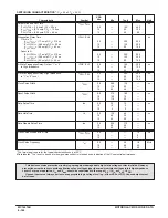
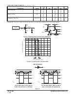
Output
Parallel Outputs
Serial Outputs
Clock
Output
Enable
Strobe
Data
Q1
QN
QS*
Q
′
S
0
X
X
Z
Z
Q7
No Chg.
0
X
X
Z
Z
No Chg.
Q7
1
0
X
No Chg.
No Chg.
Q7
No Chg.
1
1
0
0
QN–1
Q7
No Chg.
1
1
1
1
QN–1
Q7
No Chg.
1
1
1
No Chg.
No Chg.
No Chg.
Q7
Z = High Impedance
X = Don’t Care
* At the positive clock edge, information in the 7th shift register stage is transferred to
Q8 and QS.
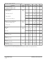
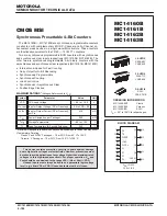
MOTOROLA
SEMICONDUCTOR TECHNICAL DATA
MC14094B
L SUFFIX
CERAMIC
CASE 620
ORDERING INFORMATION
MC14XXXBCP
Plastic
MC14XXXBCL
Ceramic
MC14XXXBD
SOIC
TA = – 55
°
to 125
°
C for all packages.
P SUFFIX
PLASTIC
CASE 648
D SUFFIX
SOIC
CASE 751B
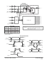
13
14
15
16
9
10
11
12
5
4
3
2
1
8
7
6
Q7
Q6
Q5
OUTPUT
ENABLE
VDD
QS
Q
′
S
Q8
Q1
CLOCK
DATA
STROBE
VSS
Q4
Q3
Q2
PIN ASSIGNMENT
This device contains protection circuitry to
guard against damage due to high static
voltages or electric fields. However, pre-
cautions must be taken to avoid applications of
any voltage higher than maximum rated volt-
ages to this high–impedance circuit. For proper
operation, Vin and Vout should be constrained
to the range VSS
v
(Vin or Vout)
v
VDD.
Unused inputs must always be tied to an
appropriate logic voltage level (e.g., either VSS
or VDD). Unused outputs must be left open.
Содержание CMOS Logic
Страница 1: ......
Страница 5: ...iv MOTOROLA CMOS LOGIC DATA ...
Страница 6: ...Master Index 1 ...
Страница 12: ...Product Selection Guide 2 ...
Страница 17: ...The Better Program 3 ...
Страница 20: ...B and UB Series Family Data 4 ...
Страница 25: ...CMOS Handling and Design Guidelines 5 ...
Страница 32: ...CMOS Handling and Design Guidelines 5 ...
Страница 39: ...Data Sheets 6 ...
Страница 69: ...MOTOROLA CMOS LOGIC DATA 6 31 MC14008B Figure 5 Logic Diagram Cin A1 B1 A2 B2 A3 B3 A4 B4 S1 S2 S3 S4 Cout ...
Страница 234: ...MOTOROLA CMOS LOGIC DATA MC14174B 6 196 FUNCTIONAL BLOCK DIAGRAM TIMING DIAGRAM ...
Страница 238: ...MOTOROLA CMOS LOGIC DATA MC14175B 6 200 FUNCTIONAL BLOCK DIAGRAM TIMING DIAGRAM ...
Страница 555: ...CMOS Reliability 7 ...
Страница 561: ...Equivalent Gate Count 8 ...
Страница 563: ...Packaging Information Including Surface Mounts 9 ...
Страница 571: ......