


MOTOROLA CMOS LOGIC DATA
MC14553B
6–416
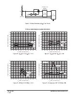
OPERATING CHARACTERISTICS
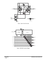
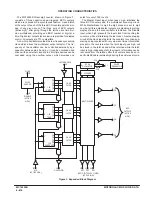
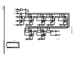
The MC14553B three–digit counter, shown in Figure 3,
consists of three negative edge–triggered BCD counters
which are cascaded in a synchronous fashion. A quad latch
at the output of each of the three BCD counters permits stor-
age of any given count. The three sets of BCD outputs
(active high), after going through the latches, are time divi-
sion multiplexed, providing one BCD number or digit at a
time. Digit select outputs (active low) are provided for display
control. All outputs are TTL compatible.
An on–chip oscillator provides the low frequency scanning
clock which drives the multiplexer output selector. The fre-
quency of the oscillator can be controlled externally by a
capacitor between pins 3 and 4, or it can be overridden and
driven with an external clock at pin 4. Multiple devices can be
cascaded using the overflow output, which provides one
pulse for every 1000 counts.
The Master Reset input, when taken high, initializes the
three BCD counters and the multiplexer scanning circuit.
While Master Reset is high the digit scanner is set to digit
one; but all three digit select outputs are disabled to prolong
display life, and the scan oscillator is inhibited. The Disable
input, when high, prevents the input clock from reaching the
counters, while still retaining the last count. A pulse shaping
circuit at the clock input permits the counters to continue op-
erating on input pulses with very slow rise times. Information
present in the counters when the latch input goes high, will
be stored in the latches and will be retained while the latch
input is high, independent of other inputs. Information can be
recovered from the latches after the counters have been re-
set if Latch Enable remains high during the entire reset cycle.
Figure 3. Expanded Block Diagram
PULSE
SHAPER
CLOCK
12
11
DISABLE
(ACTIVE
HIGH)
C
R
Q0
Q1
Q2
Q3
÷
10
UNITS
C
R
Q0
Q1
Q2
Q3
÷
10
TENS
C
R
Q0
Q1
Q2
Q3
÷
10
HUNDREDS
10
LATCH ENABLE
QUAD
LATCH
QUAD
LATCH
QUAD
LATCH
R
R
SCAN
OSCILLATOR
SCANNER
PULSE
GENERATOR
C1
4
3
C1A
C1B
MULTIPLEXER
9
7
6
5
Q0
Q1
Q2
Q3
BCD
OUTPUTS
(ACTIVE
HIGH)
13
14
2
1
15
MR
(ACTIVE HIGH)
OVERFLOW
DS1
DS2
DS3
(LSD) DIGIT SELECT (MSD)
(ACTIVE LOW)
Содержание CMOS Logic
Страница 1: ......
Страница 5: ...iv MOTOROLA CMOS LOGIC DATA ...
Страница 6: ...Master Index 1 ...
Страница 12: ...Product Selection Guide 2 ...
Страница 17: ...The Better Program 3 ...
Страница 20: ...B and UB Series Family Data 4 ...
Страница 25: ...CMOS Handling and Design Guidelines 5 ...
Страница 32: ...CMOS Handling and Design Guidelines 5 ...
Страница 39: ...Data Sheets 6 ...
Страница 69: ...MOTOROLA CMOS LOGIC DATA 6 31 MC14008B Figure 5 Logic Diagram Cin A1 B1 A2 B2 A3 B3 A4 B4 S1 S2 S3 S4 Cout ...
Страница 234: ...MOTOROLA CMOS LOGIC DATA MC14174B 6 196 FUNCTIONAL BLOCK DIAGRAM TIMING DIAGRAM ...
Страница 238: ...MOTOROLA CMOS LOGIC DATA MC14175B 6 200 FUNCTIONAL BLOCK DIAGRAM TIMING DIAGRAM ...
Страница 555: ...CMOS Reliability 7 ...
Страница 561: ...Equivalent Gate Count 8 ...
Страница 563: ...Packaging Information Including Surface Mounts 9 ...
Страница 571: ......