


MOTOROLA CMOS LOGIC DATA
6–451
MC14562B
128-Bit Static Shift Register
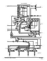
The MC14562B is a 128–bit static shift register constructed with MOS
P–channel and N–channel enhancement mode devices in a single
monolithic structure. Data is clocked in and out of the shift register on the
positive edge of the clock input. Data outputs are available every 16 bits,
from 16 through bit 128. This complementary MOS shift register is primarily
used where low power dissipation and/or high noise immunity is desired.
•
Diode Protection on All Inputs
•
Fully Static Operation
•
Cascadable to Provide Longer Shift Register Lengths
•
Supply Voltage Range = 3.0 Vdc to 18 Vdc
•
Capable of Driving Two Low–power TTL Loads or One Low–power
Schottky TTL Load Over the Rated Temperature Range
ÎÎÎÎÎÎÎÎÎÎÎÎÎÎÎÎÎÎÎÎÎ
ÎÎÎÎÎÎÎÎÎÎÎÎÎÎÎÎÎÎÎÎÎ
MAXIMUM RATINGS*
(Voltages Referenced to VSS)
Symbol
Parameter
Value
Unit
VDD
DC Supply Voltage
– 0.5 to + 18.0
V
Vin, Vout Input or Output Voltage (DC or Transient)
– 0.5 to VDD + 0.5
V
Iin, Iout
Input or Output Current (DC or Transient),
per Pin
±
10
mA
PD
Power Dissipation, per Package†
500
mW
Tstg
Storage Temperature
– 65 to + 150
_
C
TL
Lead Temperature (8–Second Soldering)
260
_
C
* Maximum Ratings are those values beyond which damage to the device may occur.
†Temperature Derating:
Plastic “P and D/DW” Packages: – 7.0 mW/
_
C From 65
_
C To 125
_
C
Ceramic “L” Packages: – 12 mW/
_
C From 100
_
C To 125
_
C
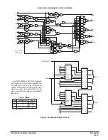
LOGIC DIAGRAM
D
C
Q
1
D
C
Q
2
D
C
Q
3
D
C
Q
16
D
C
Q
17
D
C
Q
32
D
C
Q
33
D
C
Q
48
D
C
Q
49
D
C
Q
64
CLOCK 5
DATA IN 12
D
C
Q
65
D
C
Q
80
D
C
Q
81
D
C
Q
96
D
C
Q
97
D
C
Q
112
D
C
Q
113
D
C
Q
128
10 Q16
13 Q32
9 Q48
1 Q64
8 Q80
2 Q96
6 Q112
3 Q128
MOTOROLA
SEMICONDUCTOR TECHNICAL DATA
MC14562B
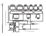
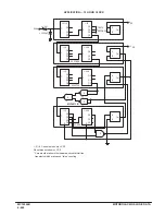
BLOCK DIAGRAM
L SUFFIX
CERAMIC
CASE 632
ORDERING INFORMATION
MC14XXXBCP
Plastic
MC14XXXBCL
Ceramic
MC14XXXBD
SOIC
TA = – 55
°
to 125
°
C for all packages.
P SUFFIX
PLASTIC
CASE 646
D SUFFIX
SOIC
CASE 751A
10
13
9
1
8
2
6
3
Q128
Q112
Q96
Q80
Q64
Q48
Q32
Q16
12
5
DATA
CLOCK
VDD = PIN 14
VSS = PIN 7
Pins 4 and 11
not used.
Содержание CMOS Logic
Страница 1: ......
Страница 5: ...iv MOTOROLA CMOS LOGIC DATA ...
Страница 6: ...Master Index 1 ...
Страница 12: ...Product Selection Guide 2 ...
Страница 17: ...The Better Program 3 ...
Страница 20: ...B and UB Series Family Data 4 ...
Страница 25: ...CMOS Handling and Design Guidelines 5 ...
Страница 32: ...CMOS Handling and Design Guidelines 5 ...
Страница 39: ...Data Sheets 6 ...
Страница 69: ...MOTOROLA CMOS LOGIC DATA 6 31 MC14008B Figure 5 Logic Diagram Cin A1 B1 A2 B2 A3 B3 A4 B4 S1 S2 S3 S4 Cout ...
Страница 234: ...MOTOROLA CMOS LOGIC DATA MC14174B 6 196 FUNCTIONAL BLOCK DIAGRAM TIMING DIAGRAM ...
Страница 238: ...MOTOROLA CMOS LOGIC DATA MC14175B 6 200 FUNCTIONAL BLOCK DIAGRAM TIMING DIAGRAM ...
Страница 555: ...CMOS Reliability 7 ...
Страница 561: ...Equivalent Gate Count 8 ...
Страница 563: ...Packaging Information Including Surface Mounts 9 ...
Страница 571: ......