


MOTOROLA CMOS LOGIC DATA
MC14490
6–214
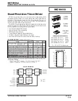
Figure 4. Typical “Form A” Contact Debounce Circuit
(Only One Debouncer Shown)
1/2 BIT
DELAY
OSCILLATOR
AND
TWO–PHASE
CLOCK GENERATOR
Cext
OSCout
OSCin
“FORM A”
CONTACT
Ain
1
9
7
φ
1
φ
2
DATA
SHIFT
LOAD
4–BIT STATIC SHIFT REGISTER
φ
1
φ
2
φ
1
φ
2
15
Aout
+VDD
PULLUP RESISTOR
(INTERNAL)
OPERATING CHARACTERISTICS
The single most important characteristic of the MC14490
is that it works with a single signal lead as an input, making
it directly compatible with mechanical contacts (Form A
and B).
The circuit has a built–in pullup resistor on each input. The
worst case value of the pullup resistor (determined from the
Electrical Characteristics table) is used to calculate the con-
tact wetting current. If more contact current is required, an
external resistor may be connected between VDD and the
input.
Because of the built–in pullup resistors, the inputs cannot
be driven with a single standard CMOS gate when VDD is be-
low 5 V. At this voltage, the input should be driven with paral-
leled standard gates or by the MC14049 or MC14050
buffers.
The clock input circuit (pin 7) has Schmitt trigger shaping
such that proper clocking will occur even with very slow clock
edges, eliminating any need for clock preshaping. In addi-
tion, other MC14490 oscillator inputs can be driven from a
single oscillator output buffered by an MC14050 (see Fig-
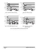
ure 5). Up to six MC14490s may be driven by a single buffer.
The MC14490 is TTL compatible on both the inputs and
the outputs. When VDD is at 4.5 V, the buffered outputs can
sink 1.6 mA at 0.4 V. The inputs can be driven with TTL as a
result of the internal input pullup resistors.
Figure 5. Typical Single Oscillator Debounce System
FROM CONTACTS
MC14490
TO SYSTEM
LOGIC
OSCin
OSCout
Cext
1/6 MC14050
9
7
OSCin 7
9 OSCout
NO CONNECTION
FROM
CONTACTS
TO SYSTEM
LOGIC
MC14490
NO CONNECTION
9 OSCout
OSCin 7
FROM CONTACTS
MC14490
TO SYSTEM
LOGIC
Содержание CMOS Logic
Страница 1: ......
Страница 5: ...iv MOTOROLA CMOS LOGIC DATA ...
Страница 6: ...Master Index 1 ...
Страница 12: ...Product Selection Guide 2 ...
Страница 17: ...The Better Program 3 ...
Страница 20: ...B and UB Series Family Data 4 ...
Страница 25: ...CMOS Handling and Design Guidelines 5 ...
Страница 32: ...CMOS Handling and Design Guidelines 5 ...
Страница 39: ...Data Sheets 6 ...
Страница 69: ...MOTOROLA CMOS LOGIC DATA 6 31 MC14008B Figure 5 Logic Diagram Cin A1 B1 A2 B2 A3 B3 A4 B4 S1 S2 S3 S4 Cout ...
Страница 234: ...MOTOROLA CMOS LOGIC DATA MC14174B 6 196 FUNCTIONAL BLOCK DIAGRAM TIMING DIAGRAM ...
Страница 238: ...MOTOROLA CMOS LOGIC DATA MC14175B 6 200 FUNCTIONAL BLOCK DIAGRAM TIMING DIAGRAM ...
Страница 555: ...CMOS Reliability 7 ...
Страница 561: ...Equivalent Gate Count 8 ...
Страница 563: ...Packaging Information Including Surface Mounts 9 ...
Страница 571: ......