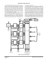


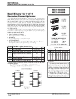

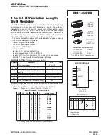


MOTOROLA CMOS LOGIC DATA
MC14558B
6–430
ÎÎÎÎÎÎÎÎÎÎÎÎÎÎÎÎÎÎÎÎÎÎÎÎÎÎÎÎÎÎÎÎÎÎ
ÎÎÎÎÎÎÎÎÎÎÎÎÎÎÎÎÎÎÎÎÎÎÎÎÎÎÎÎÎÎÎÎÎÎ
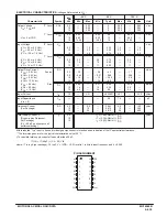
ELECTRICAL CHARACTERISTICS
(Voltages Referenced to VSS)
VDD
– 55
_
C
25
_
C
125
_
C
Characteristic
Symbol
VDD
Vdc
Min
Max
Min
Typ #
Max
Min
Max
Unit
Output Voltage
“0” Level
Vin = VDD or 0
VOL
5.0
10
15
—
—
—
0.05
0.05
0.05
—
—
—
0
0
0
0.05
0.05
0.05
—
—
—
0.05
0.05
0.05
Vdc
“1” Level
Vin = 0 or VDD
VOH
5.0
10
15
4.95
9.95
14.95
—
—
—
4.95
9.95
14.95
5.0
10
15
—
—
—
4.95
9.95
14.95
—
—
—
Vdc
Input Voltage
“0” Level
(VO = 4.5 or 0.5 Vdc)
(VO = 9.0 or 1.0 Vdc)
(VO = 13.5 or 1.5 Vdc)
VIL
5.0
10
15
—
—
—
1.5
3.0
4.0
—
—
—
2.25
4.50
6.75
1.5
3.0
4.0
—
—
—
1.5
3.0
4.0
Vdc
“1” Level
(VO = 0.5 or 4.5 Vdc)
(VO = 1.0 or 9.0 Vdc)
(VO = 1.5 or 13.5 Vdc)
VIH
5.0
10
15
3.5
7.0
11
—
—
—
3.5
7.0
11
2.75
5.50
8.25
—
—
—
3.5
7.0
11
—
—
—
Vdc
Output Drive Current
(VOH = 2.5 Vdc)
Source
(VOH = 4.6 Vdc)
(VOH = 9.5 Vdc)
(VOH = 13.5 Vdc)
IOH
5.0
5.0
10
15
– 3.0
– 0.64
– 1.6
– 4.2
—
—
—
—
– 2.4
– 0.51
– 1.3
– 3.4
– 4.2
– 0.88
– 2.25
– 8.8
—
—
—
—
– 1.7
– 0.36
– 0.9
– 2.4
—
—
—
—
mAdc
(VOL = 0.4 Vdc)
Sink
(VOL = 0.5 Vdc)
(VOL = 1.5 Vdc)
IOL
5.0
10
15
0.64
1.6
4.2
—
—
—
0.51
1.3
3.4
0.88
2.25
8.8
—
—
—
0.36
0.9
2.4
—
—
—
mAdc
Input Current
Iin
15
—
±
0.1
—
±
0.00001
±
0.1
—
±
1.0
µ
Adc
Input Capacitance
Cin
—
—
—
—
5.0
7.5
—
—
pF
Quiescent Current
(Per Package) Vin = 0 or VDD
Iout = 0
µ
A
IDD
5.0
10
15
—
—
—
5.0
10
20
—
—
—
0.005
0.010
0.015
5.0
10
20
—
—
—
150
300
600
µ
Adc
Total Supply Current**†
(Dynamic plus Quiescent,
Per Package)
(CL = 50 pF on all outputs, all
buffers switching)
IT
5.0
10
15
IT = (1.2
µ
A/kHz) f + IDD
IT = (2.4
µ
A/kHz) f + IDD
IT = (3.6
µ
A/kHz) f + IDD
µ
Adc
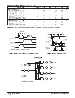
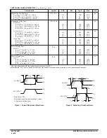
#Noise immunity specified for worst–case input combination.
Noise Margin for both “1” and “0” level = 1.0 V min @ VDD = 5.0 V
=
2.0 V min @ VDD = 10 V
=
2.5 V min @ VDD = 15 V
†To calculate total supply current at loads other than 50 pF:
IT(CL) = IT(50 pF) + 3.5 x 10⁻³ (CL – 50) VDDf
where: IT is in
µ
A (per package), CL in pF, VDD in V, and f in kHz is input frequency.
** The formulas given are for the typical characteristics only at 25
_
C.
This device contains circuitry to protect the inputs against damage due to high static voltages or electric fields; however,
it is advised that normal precautions be taken to avoid applications of any voltage higher than maximum rated voltages to this
high-impedance circuit. For proper operation it is recommended that Vin and Vout be constrained to the range VSS
≤
(Vin or
Vout)
≤
VDD.
Unused inputs must always be tied to an appropriate logic voltage level (e.g., either VSS or VDD).
Содержание CMOS Logic
Страница 1: ......
Страница 5: ...iv MOTOROLA CMOS LOGIC DATA ...
Страница 6: ...Master Index 1 ...
Страница 12: ...Product Selection Guide 2 ...
Страница 17: ...The Better Program 3 ...
Страница 20: ...B and UB Series Family Data 4 ...
Страница 25: ...CMOS Handling and Design Guidelines 5 ...
Страница 32: ...CMOS Handling and Design Guidelines 5 ...
Страница 39: ...Data Sheets 6 ...
Страница 69: ...MOTOROLA CMOS LOGIC DATA 6 31 MC14008B Figure 5 Logic Diagram Cin A1 B1 A2 B2 A3 B3 A4 B4 S1 S2 S3 S4 Cout ...
Страница 234: ...MOTOROLA CMOS LOGIC DATA MC14174B 6 196 FUNCTIONAL BLOCK DIAGRAM TIMING DIAGRAM ...
Страница 238: ...MOTOROLA CMOS LOGIC DATA MC14175B 6 200 FUNCTIONAL BLOCK DIAGRAM TIMING DIAGRAM ...
Страница 555: ...CMOS Reliability 7 ...
Страница 561: ...Equivalent Gate Count 8 ...
Страница 563: ...Packaging Information Including Surface Mounts 9 ...
Страница 571: ......