


MOTOROLA CMOS LOGIC DATA
6–97
MC14034B
8-Bit Universal Bus Register
The MC14034B is a bidirectional 8–bit static parallel/serial, input/output
bus register. The device contains two sets of input/output lines which allows
the bidirectional transfer of data between two buses; the conversion of serial
data to parallel form, or the conversion of parallel data to serial form.
Additionally the serial data input allows data to be entered shift/right, while
shift/left can be accomplished by hard–wiring each parallel output to the
previous parallel bit input.
Other useful applications for this device include pseudo–random code
generation, sample and hold register, frequency and phase–comparator,
address or buffer register, and serial/parallel input/output conversions.
•
Bidirectional Parallel Data Input
•
Diode Protection on All Inputs
•
Supply Voltage Range = 3.0 Vdc to 18 Vdc
•
Capable of Driving Two Low–power TTL Loads or One Low–power
Schottky TTL Load Over the Rated Temperature Range.
•
Pin–for–Pin Replacement for CD4034B.
ÎÎÎÎÎÎÎÎÎÎÎÎÎÎÎÎÎÎÎÎÎ
ÎÎÎÎÎÎÎÎÎÎÎÎÎÎÎÎÎÎÎÎÎ
MAXIMUM RATINGS*
(Voltages Referenced to VSS)
ÎÎÎÎ
ÎÎÎÎ
Symbol
ÎÎÎÎÎÎÎÎÎÎÎ
ÎÎÎÎÎÎÎÎÎÎÎ
Parameter
ÎÎÎÎÎÎ
ÎÎÎÎÎÎ
Value
ÎÎÎ
ÎÎÎ
Unit
ÎÎÎÎ
ÎÎÎÎ
VDD
ÎÎÎÎÎÎÎÎÎÎÎ
ÎÎÎÎÎÎÎÎÎÎÎ
DC Supply Voltage
ÎÎÎÎÎÎ
ÎÎÎÎÎÎ
– 0.5 to + 18.0
ÎÎÎ
ÎÎÎ
V
ÎÎÎÎ
ÎÎÎÎ
Vin, Vout
ÎÎÎÎÎÎÎÎÎÎÎ
ÎÎÎÎÎÎÎÎÎÎÎ
Input or Output Voltage (DC or Transient)
ÎÎÎÎÎÎ
ÎÎÎÎÎÎ
– 0.5 to VDD + 0.5
ÎÎÎ
ÎÎÎ
V
ÎÎÎÎ
ÎÎÎÎ
lin, lout
ÎÎÎÎÎÎÎÎÎÎÎ
ÎÎÎÎÎÎÎÎÎÎÎ
Input or Output Current (DC or Transient),
per Pin
ÎÎÎÎÎÎ
ÎÎÎÎÎÎ
±
10
ÎÎÎ
ÎÎÎ
mA
ÎÎÎÎ
ÎÎÎÎ
PD
ÎÎÎÎÎÎÎÎÎÎÎ
ÎÎÎÎÎÎÎÎÎÎÎ
Power Dissipation, per Package†
ÎÎÎÎÎÎ
ÎÎÎÎÎÎ
500
ÎÎÎ
ÎÎÎ
mW
ÎÎÎÎ
ÎÎÎÎ
Tstg
ÎÎÎÎÎÎÎÎÎÎÎ
ÎÎÎÎÎÎÎÎÎÎÎ
Storage Temperature
ÎÎÎÎÎÎ
ÎÎÎÎÎÎ
– 65 to + 150
ÎÎÎ
ÎÎÎ
_
C
ÎÎÎÎ
ÎÎÎÎ
TL
ÎÎÎÎÎÎÎÎÎÎÎ
ÎÎÎÎÎÎÎÎÎÎÎ
Lead Temperature (8–Second Soldering)
ÎÎÎÎÎÎ
ÎÎÎÎÎÎ
260
ÎÎÎ
ÎÎÎ
_
C
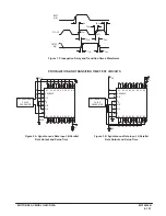
* Maximum Ratings are those values beyond which damage to the device may occur.
†Temperature Derating:
Plastic “P and D/DW” Packages: – 7.0 mW/
_
C From 65
_
C To 125
_
C
Ceramic “L” Packages: – 12 mW/
_
C From 100
_
C To 125
_
C
This device contains protection circuitry to guard against damage
due to high static voltages or electric fields. However, precautions must
be taken to avoid applications of any voltage higher than maximum rated
voltages to this high-impedance circuit. For proper operation, Vin and
Vout should be constrained to the range VSS
≤
(Vin or Vout)
≤
VDD.
Unused inputs must always be tied to an appropriate logic voltage
level (e.g., either VSS or VDD). Unused outputs must be left open.
MOTOROLA
SEMICONDUCTOR TECHNICAL DATA
MC14034B
L SUFFIX
CERAMIC
CASE 623
ORDERING INFORMATION
MC14XXXBCP
Plastic
MC14XXXBCL
Ceramic
MC14XXXBDW
SOIC
TA = – 55
°
to 125
°
C for all packages.
P SUFFIX
PLASTIC
CASE 709
DW SUFFIX
SOIC
CASE 751E
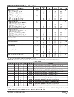
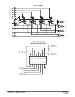
PIN ASSIGNMENT
B3
B5
B6
B7
B8
B1
B2
B4
A5
A6
A7
A8
VDD
C
A1
A2
5
4
3
2
1
10
9
8
7
6
14
15
16
17
18
19
20
13
11
12
21
22
23
24
P/S
A/S
A3
A4
A/B
VSS
DS
A ENABLE
Содержание CMOS Logic
Страница 1: ......
Страница 5: ...iv MOTOROLA CMOS LOGIC DATA ...
Страница 6: ...Master Index 1 ...
Страница 12: ...Product Selection Guide 2 ...
Страница 17: ...The Better Program 3 ...
Страница 20: ...B and UB Series Family Data 4 ...
Страница 25: ...CMOS Handling and Design Guidelines 5 ...
Страница 32: ...CMOS Handling and Design Guidelines 5 ...
Страница 39: ...Data Sheets 6 ...
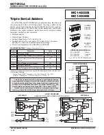
Страница 69: ...MOTOROLA CMOS LOGIC DATA 6 31 MC14008B Figure 5 Logic Diagram Cin A1 B1 A2 B2 A3 B3 A4 B4 S1 S2 S3 S4 Cout ...
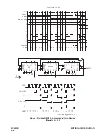
Страница 234: ...MOTOROLA CMOS LOGIC DATA MC14174B 6 196 FUNCTIONAL BLOCK DIAGRAM TIMING DIAGRAM ...
Страница 238: ...MOTOROLA CMOS LOGIC DATA MC14175B 6 200 FUNCTIONAL BLOCK DIAGRAM TIMING DIAGRAM ...
Страница 555: ...CMOS Reliability 7 ...
Страница 561: ...Equivalent Gate Count 8 ...
Страница 563: ...Packaging Information Including Surface Mounts 9 ...
Страница 571: ......