


MOTOROLA CMOS LOGIC DATA
MC14538B
6–370
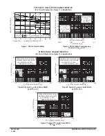
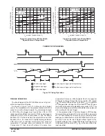
Figure 8. Typical Error of Pulse Width
Equation versus Temperature
Figure 9. Typical Error of Pulse Width
Equation versus Temperature
– 2
– 1
0
1
2
– 60 – 40
– 20
0
20
40
60
80
100
120
140
TA, AMBIENT TEMPERATURE (
°
C)
TYPICAL
NORMALIZED ERROR
WITH RESPECT
T
O
25
DD
= 10 V (%)
°
C V
ALUE
A
T
V
RX = 100 k
Ω
CX = 0.1
µ
F
VDD = 15 V
VDD = 10 V
VDD = 5 V
– 2.0
– 1.0
0
1.0
2.0
3.0
– 3.0
– 60 – 40
– 20
0
20
40
60
80
100
120
140
TA, AMBIENT TEMPERATURE (
°
C)
RX = 100 k
Ω
CX = .002
µ
F
VDD = 15 V
VDD = 10 V
VDD = 5.0 V
TYPICAL
NORMALIZED ERROR
WITH RESPECT
T
O
25
DD
= 10 V (%)
°
C V
ALUE
A
T
V
THEORY OF OPERATION
2
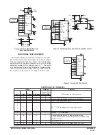
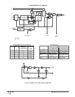
Figure 10. Timing Operation
Positive edge re–trigger (pulse lengthening)
Positive edge trigger
1
2
3
4
5
1
3
4
5
RESET
A
B
CX/RX
Q
Vref 1
Vref 1
Vref 1
Vref 1
Vref 2
Vref 2
Vref 2
Vref 2
T
T
T
Negative edge trigger
Positive edge trigger
Positive edge re–trigger (pulse lengthening)
TRIGGER OPERATION
The block diagram of the MC14538B is shown in Figure 1,
with circuit operation following.
As shown in Figure 1 and 10, before an input trigger
occurs, the monostable is in the quiescent state with the Q
output low, and the timing capacitor CX completely charged
to VDD. When the trigger input A goes from VSS to VDD
(while inputs B and Reset are held to VDD) a valid trigger is
recognized, which turns on comparator C1 and N–channel
transistor N1
➀
. At the same time the output latch is set. With
transistor N1 on, the capacitor CX rapidly discharges toward
VSS until Vref1 is reached. At this point the output of
comparator C1 changes state and transistor N1 turns off.
Comparator C1 then turns off while at the same time
comparator C2 turns on. With transistor N1 off, the capacitor
CX begins to charge through the timing resistor, RX, toward
VDD. When the voltage across CX equals Vref 2, comparator
C2 changes state, causing the output latch to reset (Q goes
low) while at the same time disabling comparator C2
➁
. This
ends at the timing cycle with the monostable in the quiescent
state, waiting for the next trigger.
In the quiescent state, CX is fully charged to VDD causing
the current through resistor RX to be zero. Both comparators
are “off” with total device current due only to reverse junction
leakages. An added feature of the MC14538B is that the out-
put latch is set via the input trigger without regard to the
capacitor voltage. Thus, propagation delay from trigger to Q
is independent of the value of CX, RX, or the duty cycle of the
input waveform.
Содержание CMOS Logic
Страница 1: ......
Страница 5: ...iv MOTOROLA CMOS LOGIC DATA ...
Страница 6: ...Master Index 1 ...
Страница 12: ...Product Selection Guide 2 ...
Страница 17: ...The Better Program 3 ...
Страница 20: ...B and UB Series Family Data 4 ...
Страница 25: ...CMOS Handling and Design Guidelines 5 ...
Страница 32: ...CMOS Handling and Design Guidelines 5 ...
Страница 39: ...Data Sheets 6 ...
Страница 69: ...MOTOROLA CMOS LOGIC DATA 6 31 MC14008B Figure 5 Logic Diagram Cin A1 B1 A2 B2 A3 B3 A4 B4 S1 S2 S3 S4 Cout ...
Страница 234: ...MOTOROLA CMOS LOGIC DATA MC14174B 6 196 FUNCTIONAL BLOCK DIAGRAM TIMING DIAGRAM ...
Страница 238: ...MOTOROLA CMOS LOGIC DATA MC14175B 6 200 FUNCTIONAL BLOCK DIAGRAM TIMING DIAGRAM ...
Страница 555: ...CMOS Reliability 7 ...
Страница 561: ...Equivalent Gate Count 8 ...
Страница 563: ...Packaging Information Including Surface Mounts 9 ...
Страница 571: ......