


MOTOROLA CMOS LOGIC DATA
MC14049UB
6–132
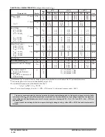
Figure 2. Typical Output Source Characteristics
Figure 3. Typical Output Sink Characteristics
VDD
VSS
1
8
IOH
VOH
VDS = VOH – VDD
VDD
VSS
1
8
IOL
VOL
VDD = VOL
I OH
, OUTPUT
SOURCE CURRNT
(mAdc)
I OL
, OUTPUT
SINK CURRENT
(mAdc)
– 50
– 40
– 30
– 20
– 10
0
– 10
– 8.0
– 6.0
– 4.0
– 2.0
0
VDS, DRAIN–TO–SOURCE VOLTAGE (Vdc)
VGS = 5.0 Vdc
VGS = 10 Vdc
MAXIMUM CURRENT LEVEL
VGS = 15 Vdc
160
120
80
40
0
0
2.0
4.0
6.0
8.0
10
VDS, DRAIN–TO–SOURCE VOLTAGE (Vdc)
VGS = 15 Vdc
VGS = 10 Vdc
MAXIMUM CURRENT LEVEL
VGS = 5.0 Vdc
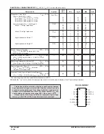
Figure 4. Ambient Temperature Power Derating
P
D
, MAXIMUM POWER DISSIP
A
TION (mW)
PER P
ACKAGE
1200
1100
1000
900
825
800
740
700
600
500
400
300
200
100
0
175
150
125
100
75
50
25
TA, AMBIENT TEMPERATURE (
°
C)
260 mW (L)
175 mW (P)
120 mW (D)
(L) CERAMIC
(P) PDIP
(D) SOIC
PULSE
GENERATOR
VDD
VSS
8
1
CL
Vout
Vin
20 ns
20 ns
VDD
VSS
VOH
VOL
90%
50%
10%
90%
50%
10%
tPLH
tTLH
tTHL
tPHL
OUTPUT
INPUT
Figure 5. Switching Time Test Circuit
and Waveforms
This device contains circuitry to protect the inputs against damage
due to high static voltages or electric fields referenced to the VSS pin,
only. Extra precautions must be taken to avoid applications of any volt-
age higher than the maximum rated voltages to this high-impedance cir-
cuit. For proper operation, the ranges VSS
≤
Vin
≤
18 V and VSS
≤
Vout
≤
VDD
are recommended.
Unused inputs must always be tied to an appropriate logic voltage
level (e.g., either VSS or VDD). Unused outputs must be left open.
PIN ASSIGNMENT
13
14
15
16
9
10
11
12
5
4
3
2
1
8
7
6
OUTE
NC
INF
OUTF
NC
IND
OUTD
INE
OUTB
INA
OUTA
VDD
VSS
INC
OUTC
INB
NC = NO CONNECTION
Содержание CMOS Logic
Страница 1: ......
Страница 5: ...iv MOTOROLA CMOS LOGIC DATA ...
Страница 6: ...Master Index 1 ...
Страница 12: ...Product Selection Guide 2 ...
Страница 17: ...The Better Program 3 ...
Страница 20: ...B and UB Series Family Data 4 ...
Страница 25: ...CMOS Handling and Design Guidelines 5 ...
Страница 32: ...CMOS Handling and Design Guidelines 5 ...
Страница 39: ...Data Sheets 6 ...
Страница 69: ...MOTOROLA CMOS LOGIC DATA 6 31 MC14008B Figure 5 Logic Diagram Cin A1 B1 A2 B2 A3 B3 A4 B4 S1 S2 S3 S4 Cout ...
Страница 234: ...MOTOROLA CMOS LOGIC DATA MC14174B 6 196 FUNCTIONAL BLOCK DIAGRAM TIMING DIAGRAM ...
Страница 238: ...MOTOROLA CMOS LOGIC DATA MC14175B 6 200 FUNCTIONAL BLOCK DIAGRAM TIMING DIAGRAM ...
Страница 555: ...CMOS Reliability 7 ...
Страница 561: ...Equivalent Gate Count 8 ...
Страница 563: ...Packaging Information Including Surface Mounts 9 ...
Страница 571: ......