


5–3
CHAPTER 5
MOTOROLA CMOS LOGIC DATA
11. The following steps should be observed during wave
solder operations:
a. The solder pot and conductive conveyor system of
the wave soldering machine must be grounded to an
earth ground.
b. The loading and unloading work benches should
have conductive tops which are grounded to an earth
ground.
c. Operators must comply with precautions previously
explained.
d. Completed assemblies should be placed in antistatic
containers prior to being moved to subsequent
stations.
12. The following steps should be observed during board–
cleaning operations:
a. Vapor degreasers and baskets must be grounded to
an earth ground.
b. Brush or spray cleaning should not be used.
c. Assemblies should be placed into the vapor
degreaser immediately upon removal from the
antistatic container.
d. Cleaned assemblies should be placed in antistatic
containers immediately after removal from the clean-
ing basket.
e. High velocity air movement or application of solvents
and coatings should be employed only when
assembled printed circuit boards are grounded and
a static eliminator is directed at the board.
13. The use of static detection meters for production line
surveillance is highly recommended.
14. Equipment specifications should alert users to the pres-
ence of CMOS devices and require familiarization with
this specification prior to performing any kind of mainte-
nance or replacement of devices or modules.
15. Do not insert or remove CMOS devices from test
sockets with power applied. Check all power supplies to
be used for testing devices to be certain there are no
voltage transients present.
16. Double check test equipment setup for proper polarity
of VDD and VSS before conducting parametric or func-
tional testing.
17. Do not recycle shipping rails or trays. Repeated use
causes deterioration of their antistatic coating.
RECOMMENDED FOR READING:
“Total Control of the Static in Your Business”
Available by writing to:
3M Company
Static Control Systems
P.O. Box 2963
Austin, Texas 78769–2963
Or by Calling:
1–800–328–1368
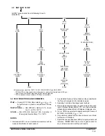
Figure 1. Networks for Minimizing ESD and Reducing
CMOS Latch Up Susceptibility
TO OFF–BOARD
CONNECTION
R1
CMOS
INPUT
OR
OUTPUT
TO OFF–BOARD
CONNECTION
CMOS
INPUT
OR
OUTPUT
R2
VDD
D1
D2
VSS
Advantage:
Disadvantage:
Requires minimal board area
R1 > R2 for the same level of
protection, therefore rise and fall
times, propagation delays, and output
drives are severely affected.
Advantage:
Disadvantage:
R2 < R1 for the same
level of protection.
Impact on ac and dc
characteristics is minimized
More board area, higher initial cost
Note: These networks are useful for protecting the following
A
B
digital inputs and outputs
analog inputs and outputs
C
D
3–state outputs
bidirectional (I/O) ports
PROPAGATION DELAY AND RISE TIME
vs. SERIES RESISTANCE
R
[
t
C
@
k
where:
R
t
C
k
k
= the maximum allowable series resistance in ohms
= the maximum tolerable propagation delay or rise time in seconds
= the board capacitance plus the driven device’s
=
input capacitance in farads
= 0.7 for propagation delay calculations
= 2.3 for rise time calculations
Содержание CMOS Logic
Страница 1: ......
Страница 5: ...iv MOTOROLA CMOS LOGIC DATA ...
Страница 6: ...Master Index 1 ...
Страница 12: ...Product Selection Guide 2 ...
Страница 17: ...The Better Program 3 ...
Страница 20: ...B and UB Series Family Data 4 ...
Страница 25: ...CMOS Handling and Design Guidelines 5 ...
Страница 32: ...CMOS Handling and Design Guidelines 5 ...
Страница 39: ...Data Sheets 6 ...
Страница 69: ...MOTOROLA CMOS LOGIC DATA 6 31 MC14008B Figure 5 Logic Diagram Cin A1 B1 A2 B2 A3 B3 A4 B4 S1 S2 S3 S4 Cout ...
Страница 234: ...MOTOROLA CMOS LOGIC DATA MC14174B 6 196 FUNCTIONAL BLOCK DIAGRAM TIMING DIAGRAM ...
Страница 238: ...MOTOROLA CMOS LOGIC DATA MC14175B 6 200 FUNCTIONAL BLOCK DIAGRAM TIMING DIAGRAM ...
Страница 555: ...CMOS Reliability 7 ...
Страница 561: ...Equivalent Gate Count 8 ...
Страница 563: ...Packaging Information Including Surface Mounts 9 ...
Страница 571: ......