background image

109

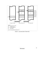
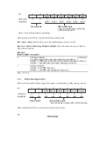
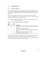
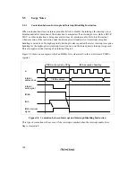
Figure 5.3 shows the timing of the setting of the interrupt flags (IRQnF).

φ

IRQn

IRQnF

input pin

Note:  n = 5 to 0

Figure 5.3   Timing of Setting of IRQnF

Interrupts IRQ

0

 to IRQ

5

 have vector numbers 12 to 17. These interrupts are detected regardless of

whether the corresponding pin is set for input or output. When using a pin for external interrupt
input, clear its DDR bit to 0 and do not use the pin for chip select output, SCI input/output, or A/D
external trigger input.

5.3.2

Internal Interrupts

27 internal interrupts are requested from the on-chip supporting modules.

• 

Each on-chip supporting module has status flags for indicating interrupt status, and enable bits
for enabling or disabling interrupts.

• 

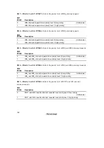
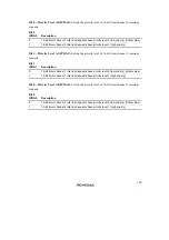
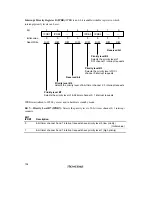
Interrupt priority levels can be assigned in IPRA and IPRB.

5.3.3

Interrupt Exception Handling Vector Table

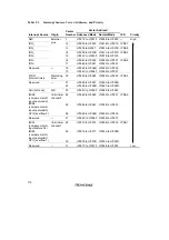
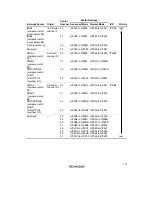
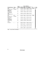
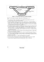
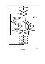
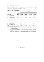
Table 5.3 lists the interrupt exception handling sources, their vector addresses, and their default
priority order. In the default priority order, smaller vector numbers have higher priority. The
priority of interrupts other than NMI can be changed in IPRA and IPRB. The priority order after a
reset is the default order shown in table 5.3.

Содержание H8/3060

Страница 1: ...etc Accordingly although Hitachi Hitachi Ltd Hitachi Semiconductors and other Hitachi brand names are mentioned in the document these names have in fact all been changed to Renesas Technology Corp Thank you for your understanding Except for our corporate trademark logo and corporate statement no changes whatsoever have been made to the contents of the document and these changes do not constitute a...

Страница 2: ...bed here may contain technical inaccuracies or typographical errors Renesas Technology Corporation assumes no responsibility for any damage liability or other loss rising from these inaccuracies or errors Please also pay attention to information published by Renesas Technology Corporation by various means including the Renesas Technology Corporation Semiconductor home page http www renesas com 4 W...

Страница 3: ...1B HD6433061B H8 3060B HD6433060B H8 3062F ZTAT HD64F3062 HD64F3062R HD64F3062B H8 3064F ZTAT HD64F3064B Hardware Manual ADE 602 136D Rev 5 0 3 18 03 Hitachi Ltd The revision list can be viewed directly by clicking the title page The revision list summarizes the locations of revisions and additions Details should always be checked by referring to the relevant text ...

Страница 4: ...of bodily injury such as aerospace aeronautics nuclear power combustion control transportation traffic safety equipment or medical equipment for life support 4 Design your application so that the product is used within the ranges guaranteed by Hitachi particularly for maximum rating operating supply voltage range heat radiation characteristics installation conditions and other characteristics Hita...

Страница 5: ...king the design of an application system using the H8 3062 Series Readers using this manual require a basic knowledge of electrical circuits logic circuits and microcomputers Purpose The purpose of this manual is to give users an understanding of the hardware functions and electrical characteristics of the H8 3062 Series Details of execution instructions can be found in the H8 300H Series Programm...

Страница 6: ...ge Editor User s Manual ADE 702 247 H8S H8 300 Series Simulator Debugger User s Manual ADE 702 037 Hitachi Embedded Workshop User s Manual ADE 702 201 H8S H8 300 Series Hitachi Embedded Workshop Hitachi Debugging Interface User s Manual ADE 702 231 Application Note Manual Title ADE No H8 300H for CPU Application Note ADE 502 033 H8 300H On Chip Supporting Modules Application Note ADE 502 035 H8 30...

Страница 7: ...T version with address output functions added Mask ROM version On chip large capacity single power supply flash memory Internal step down circuit H8 3062F ZTAT high speed operation version Mask ROM version Product code HD64F3062 HD64F3062R HD6433062 HD6433061 HD6433060 HD64F3064B HD64F3062B HD6433064B HD6433062B HD6433061B HD6433060B Pin arrange ment See figures 1 2 and 1 3 Pin Arrangement in sect...

Страница 8: ...bytes Address output functions Compatible with previous H8 300H Series Address update mode 1 or 2 selectable See 6 3 5 Address Output Method in section 6 Flash memory See section 17 ROM See 18 1 1 Differences between H8 3062F ZTAT and H8 3062F ZTAT R Mask Version in section 18 See 19 1 1 Differences between H8 3062F ZTAT and H8 3062F ZTAT R Mask Version in section 19 Mask ROM See section 17 ROM Ma...

Страница 9: ...n of H8 3062 Series Internal I O Register Specifications in appendix B See appendix B 1 Address List See appendix B 1 Address List See appendix B 1 Address List See appendix B 2 Address List See appendix B 3 Address List Mask ROM B mask version of H8 3064 see appendix B 2 Address List Mask ROM B mask versions of H8 3062 H8 3061 and H8 3060 see appendix B 3 Address List Usage notes See 1 4 H8 3062F...

Страница 10: ......

Страница 11: ...uct Type Names and Markings Table 1 7 Differences in H8 3062F ZTAT R Mask Version H8 3062F ZTAT B Mask Version H8 3064F ZTAT and H8 3064F ZTAT B Mask Version Markings The marking examples of H8 3062F ZTAT B mask version and H8 3064F ZTAT B mask version are amended 27 1 5 4 Notes on Changeover to Mask ROM Version or Mask ROM B Mask Version Title is amended Note 2 is added 6 Bus Controller 139 6 3 1...

Страница 12: ... Version 523 to 574 All The title of the section is changed from Flash Memory H8 3064F ZTAT B Mask Version 572 18 12 Mask ROM H8 3064 Mask ROM B Mask Version Overview Newly added 573 18 13 Notes on Ordering Mask ROM Version Chips 574 18 14 Notes on Converting the F ZTAT Application Software to the Mask ROM Versions 19 H8 3062 Internal Voltage Step Down Version ROM H8 3062F ZTAT B Mask Version Mask...

Страница 13: ...Resonator Table 20 1 1 Damping Resistance Value Note is amended 634 20 5 3 Usage Notes Table 20 7 Comparison of H8 3062 Series Operating Frequency Ranges is amended 21 Power Down State 644 21 4 3 Selection of Waiting Time for Exit from Software Standby Mode Table 21 3 Clock Frequency and Waiting Time for Clock to Settle The value 13 1 is specified for the recommended setting for DIV 1 DIV0 1 and 3...

Страница 14: ...ry Characteristics Table 22 30 Flash Memory Characteristics A new condition is added 711 to 723 22 4 Electrical Characteristics of H8 3064 Mask ROM B Mask Version Newly added 724 to 739 22 5 Electrical Characteristics of H8 3062F ZTAT B Mask Version The section is moved from 22 4 724 22 5 1 Absolute Maximum Ratings Table 22 40 Absolute Maximum Ratings The operating temperature rating is amended 72...

Страница 15: ...s added 738 22 5 6 Flash Memory Characteristics Table 22 49 Flash Memory Characteristics A new condition is added 740 to 752 22 6 Electrical Characteristics of H8 3062 Mask ROM B Mask Version H8 3061 Mask ROM B Mask Version and H8 3060 Mask ROM B Mask Version Newly added 753 to 761 22 7 Operational Timing The section is moved from 22 5 Appendix 906 C 7 Port 7 Block Diagram Figure C 7 a Port 7 Bloc...

Страница 16: ......

Страница 17: ...B Mask Version 24 1 5 1 Pin Arrangement 25 1 5 2 Product Type Names and Markings 25 1 5 3 VCL Pin 26 1 5 4 Notes on Changeover to On Chip Mask ROM Versions and On Chip Mask ROM B Mask Versions 27 1 6 Setting Oscillation Settling Wait Time 28 1 7 Caution on Crystal Resonator Connection 28 Section 2 CPU 29 2 1 Overview 29 2 1 1 Features 29 2 1 2 Differences from H8 300 CPU 30 2 2 CPU Operating Modes...

Страница 18: ...2 On Chip Memory Access Timing 63 2 9 3 On Chip Supporting Module Access Timing 64 2 9 4 Access to External Address Space 65 Section 3 MCU Operating Modes 67 3 1 Overview 67 3 1 1 Operating Mode Selection 67 3 1 2 Register Configuration 68 3 2 Mode Control Register MDCR 68 3 3 System Control Register SYSCR 69 3 4 Operating Mode Descriptions 72 3 4 1 Mode 1 72 3 4 2 Mode 2 72 3 4 3 Mode 3 72 3 4 4 ...

Страница 19: ...Register IER 106 5 2 5 IRQ Sense Control Register ISCR 107 5 3 Interrupt Sources 108 5 3 1 External Interrupts 108 5 3 2 Internal Interrupts 109 5 3 3 Interrupt Exception Handling Vector Table 109 5 4 Interrupt Operation 113 5 4 1 Interrupt Handling Process 113 5 4 2 Interrupt Exception Handling Sequence 118 5 4 3 Interrupt Response Time 119 5 5 Usage Notes 120 5 5 1 Contention between Interrupt a...

Страница 20: ...Data Size and Data Alignment 145 6 4 3 Valid Strobes 146 6 4 4 Memory Areas 147 6 4 5 Basic Bus Control Signal Timing 148 6 4 6 Wait Control 155 6 5 Idle Cycle 157 6 5 1 Operation 157 6 5 2 Pin States in Idle Cycle 159 6 6 Bus Arbiter 159 6 6 1 Operation 160 6 7 Register and Pin Input Timing 162 6 7 1 Register Write Timing 162 6 7 2 BREQ Pin Input Timing 163 Section 7 I O Ports 165 7 1 Overview 16...

Страница 21: ... Features 221 8 1 2 Block Diagrams 223 8 1 3 Pin Configuration 226 8 1 4 Register Configuration 227 8 2 Register Descriptions 228 8 2 1 Timer Start Register TSTR 228 8 2 2 Timer Synchro Register TSNC 229 8 2 3 Timer Mode Register TMDR 230 8 2 4 Timer Interrupt Status Register A TISRA 233 8 2 5 Timer Interrupt Status Register B TISRB 235 8 2 6 Timer Interrupt Status Register C TISRC 238 8 2 7 Timer...

Страница 22: ...Timer Control Register 8TCR 293 9 2 5 Timer Control Status Registers 8TCSR 296 9 3 CPU Interface 301 9 3 1 8 Bit Registers 301 9 4 Operation 303 9 4 1 8TCNT Count Timing 303 9 4 2 Compare Match Timing 304 9 4 3 Input Capture Signal Timing 305 9 4 4 Timing of Status Flag Setting 306 9 4 5 Operation with Cascaded Connection 307 9 4 6 Input Capture Setting 310 9 5 Interrupt 311 9 5 1 Interrupt Source...

Страница 23: ...r PBDR 328 10 2 5 Next Data Register A NDRA 329 10 2 6 Next Data Register B NDRB 331 10 2 7 Next Data Enable Register A NDERA 333 10 2 8 Next Data Enable Register B NDERB 334 10 2 9 TPC Output Control Register TPCR 335 10 2 10 TPC Output Mode Register TPMR 337 10 3 Operation 339 10 3 1 Overview 339 10 3 2 Output Timing 340 10 3 3 Normal TPC Output 341 10 3 4 Non Overlapping TPC Output 343 10 3 5 T...

Страница 24: ...366 12 2 3 Transmit Shift Register TSR 367 12 2 4 Transmit Data Register TDR 367 12 2 5 Serial Mode Register SMR 368 12 2 6 Serial Control Register SCR 371 12 2 7 Serial Status Register SSR 375 12 2 8 Bit Rate Register BRR 380 12 3 Operation 388 12 3 1 Overview 388 12 3 2 Operation in Asynchronous Mode 391 12 3 3 Multiprocessor Communication 400 12 3 4 Synchronous Operation 407 12 4 SCI Interrupts...

Страница 25: ...14 2 2 A D Control Status Register ADCSR 451 14 2 3 A D Control Register ADCR 453 14 3 CPU Interface 454 14 4 Operation 456 14 4 1 Single Mode SCAN 0 456 14 4 2 Scan Mode SCAN 1 458 14 4 3 Input Sampling and A D Conversion Time 460 14 4 4 External Trigger Input Timing 461 14 5 Interrupts 462 14 6 Usage Notes 462 Section 15 D A Converter 467 15 1 Overview 467 15 1 1 Features 467 15 1 2 Block Diagra...

Страница 26: ...ard Programming Mode 490 17 4 1 Boot Mode 493 17 4 2 User Program Mode 498 17 5 Flash Memory Programming Erasing 500 17 5 1 Program Mode 501 17 5 2 Program Verify Mode 502 17 5 3 Erase Mode 504 17 5 4 Erase Verify Mode 504 17 6 Flash Memory Protection 506 17 6 1 Hardware Protection 506 17 6 2 Software Protection 508 17 6 3 Error Protection 508 17 6 4 NMI Input Disabling Conditions 510 17 7 Flash M...

Страница 27: ...ry Emulation in RAM 539 18 4 4 Block Configuration 540 18 5 On Board Programming Mode 541 18 5 1 Boot Mode 542 18 5 2 User Program Mode 547 18 6 Flash Memory Programming Erasing 549 18 6 1 Program Mode 551 18 6 2 Program Verify Mode 552 18 6 3 Erase Mode 556 18 6 4 Erase Verify Mode 556 18 7 Flash Memory Protection 558 18 7 1 Hardware Protection 558 18 7 2 Software Protection 559 18 7 3 Error Prot...

Страница 28: ...iguration 592 19 5 On Board Programming Mode 593 19 5 1 Boot Mode 594 19 5 2 User Program Mode 599 19 6 Flash Memory Programming Erasing 601 19 6 1 Program Mode 603 19 6 2 Program Verify Mode 604 19 6 3 Erase Mode 608 19 6 4 Erase Verify Mode 608 19 7 Flash Memory Protection 610 19 7 1 Hardware Protection 610 19 7 2 Software Protection 611 19 7 3 Error Protection 611 19 8 Flash Memory Emulation in...

Страница 29: ...21 4 Software Standby Mode 642 21 4 1 Transition to Software Standby Mode 642 21 4 2 Exit from Software Standby Mode 643 21 4 3 Selection of Waiting Time for Exit from Software Standby Mode 643 21 4 4 Sample Application of Software Standby Mode 645 21 4 5 Usage Note 645 21 4 6 Cautions on Clearing the software Standby Mode of F ZTAT Version 646 21 5 Hardware Standby Mode 647 21 5 1 Transition to H...

Страница 30: ...ics of H8 3064 Mask ROM B Mask Version 711 22 4 1 Absolute Maximum Ratings 711 22 4 2 DC Characteristics 712 22 4 3 AC Characteristics 716 22 4 4 A D Conversion Characteristics 722 22 4 5 D A Conversion Characteristics 723 22 5 Electrical Characteristics of H8 3062F ZTAT B Mask Version 724 22 5 1 Absolute Maximum Ratings 724 22 5 2 DC Characteristics 725 22 5 3 AC Characteristics 730 22 5 4 A D Co...

Страница 31: ...062 Mask ROM B Mask Version H8 3061 Mask ROM B Mask Version and H8 3060 Mask ROM B Mask Version 811 B 4 Functions 821 Appendix C I O Port Block Diagrams 896 C 1 Port 1 Block Diagram 896 C 2 Port 2 Block Diagram 897 C 3 Port 3 Block Diagram 898 C 4 Port 4 Block Diagram 899 C 5 Port 5 Block Diagram 900 C 6 Port 6 Block Diagrams 901 C 7 Port 7 Block Diagrams 906 C 8 Port 8 Block Diagrams 907 C 9 Port...

Страница 32: ...of H8 300H Series Product Specifications 939 H 1 Differences between H8 3067 and H8 3062 Series H8 3048 Series H8 3007 and H8 3006 and H8 3002 939 H 2 Comparison of Pin Functions of 100 Pin Package Products FP 100B TFP 100B 942 ...

Страница 33: ...062F ZTAT B Mask Version H8 3064F ZTAT B Mask Version and On Chip Mask ROM B Mask Versions 26 Figure 1 7 Example of Board Pattern Providing for External Capacitor 27 Figure 2 1 CPU Operating Modes 31 Figure 2 2 Memory Map 31 Figure 2 3 CPU Registers 32 Figure 2 4 Usage of General Registers 33 Figure 2 5 Stack 34 Figure 2 6 General Register Data Formats 36 Figure 2 7 General Register Data Formats 3...

Страница 34: ...rrupt Disabling Instruction 120 Figure 6 1 Block Diagram of Bus Controller 124 Figure 6 2 Access Area Map for Each Operating Mode 137 Figure 6 3 Memory Map in 16 Mbyte Mode H8 3062F ZTAT H8 3062F ZTAT B Mask Version H8 3062 Mask ROM Version H8 3061 Mask ROM Version H8 3062 Mask ROM B Mask Version H8 3061 Mask ROM B Mask Version 1 138 Figure 6 3 Memory Map in 16 Mbyte Mode H8 3060 Mask ROM Version ...

Страница 35: ... 181 Figure 7 6 Port 6 Pin Configuration 185 Figure 7 7 Port 7 Pin Configuration 188 Figure 7 8 Port 8 Pin Configuration 190 Figure 7 9 Port 9 Pin Configuration 195 Figure 7 10 Port A Pin Configuration 201 Figure 7 11 Port B Pin Configuration 213 Figure 8 1 16 bit timer Block Diagram Overall 223 Figure 8 2 Block Diagram of Channels 0 and 1 224 Figure 8 3 Block Diagram of Channel 2 225 Figure 8 4 1...

Страница 36: ...8 Contention between 16TCNT Word Write and Increment 273 Figure 8 39 Contention between 16TCNT Byte Write and Increment 274 Figure 8 40 Contention between General Register Write and Compare Match 275 Figure 8 41 Contention between 16TCNT Write and Overflow 276 Figure 8 42 Contention between General Register Read and Input Capture 277 Figure 8 43 Contention between Counter Clearing by Input Capture...

Страница 37: ...Figure 10 8 TPC Output Triggering by Input Capture Example 345 Figure 10 9 Non Overlapping TPC Output 346 Figure 10 10 Non Overlapping Operation and NDR Write Timing 347 Figure 11 1 WDT Block Diagram 350 Figure 11 2 Format of Data Written to TCNT and TCSR 355 Figure 11 3 Format of Data Written to RSTCSR 356 Figure 11 4 Operation in Watchdog Timer Mode 357 Figure 11 5 Interval Timer Operation 358 F...

Страница 38: ...am of Smart Card Interface 422 Figure 13 2 Smart Card Interface Connection Diagram 430 Figure 13 3 Smart Card Interface Data Format 431 Figure 13 4 Timing of TEND Flag Setting 437 Figure 13 5 Sample Transmission Processing Flowchart 438 Figure 13 6 Relation Between Transmit Operation and Internal Registers 439 Figure 13 7 Timing of TEND Flag Setting 439 Figure 13 8 Sample Reception Processing Flow...

Страница 39: ...On Off Timing User Program Mode 518 Figure 17 18 Mode Transition Timing Example Boot Mode User Mode User Program Mode 519 Figure 17 19 ROM Block Diagram H8 3062 Mask ROM Version 520 Figure 17 20 Mask ROM Addresses and Data 521 Figure 18 1 Block Diagram of Flash Memory 526 Figure 18 2 Flash Memory Related State Transitions 536 Figure 18 3 Reading Overlap RAM Data in User Mode User Program Mode 539 ...

Страница 40: ...4 Example of RAM Overlap Operation 614 Figure 19 15 Memory Map in PROM Mode 617 Figure 19 16 Power On Off Timing Boot Mode 621 Figure 19 17 Power On Off Timing User Program Mode 622 Figure 19 18 Mode Transition Timing Example Boot Mode User Mode User Program Mode 623 Figure 19 19 ROM Block Diagram H8 3062 Mask ROM B Mask Version 624 Figure 19 20 Mask ROM Addresses and Data 625 Figure 20 1 Block Di...

Страница 41: ...utput Timing 760 Figure 22 28 Timer Input Output Timing 760 Figure 22 29 Timer External Clock Input Timing 761 Figure 22 30 SCI Input Clock Timing 761 Figure 22 31 SCI Input Output Timing in Synchronous Mode 761 Figure C 1 Port 1 Block Diagram 896 Figure C 2 Port 2 Block Diagram 897 Figure C 3 Port 3 Block Diagram 898 Figure C 4 Port 4 Block Diagram 899 Figure C 5 Port 5 Block Diagram 900 Figure C...

Страница 42: ... 11 b Port B Block Diagram Pins PB1 and PB3 921 Figure C 11 c Port B Block Diagram Pin PB4 922 Figure C 11 d Port B Block Diagram Pin PB5 923 Figure C 11 e Port B Block Diagram Pin PB6 924 Figure C 11 f Port B Block Diagram Pin PB7 925 Figure D 1 Reset during Memory Access Modes 1 and 2 930 Figure D 2 Reset during Memory Access Modes 3 and 4 931 Figure D 3 Reset during Memory Access Mode 5 932 Fig...

Страница 43: ...46 Table 2 8 Branching Instructions 48 Table 2 9 System Control Instructions 49 Table 2 10 Block Transfer Instruction 50 Table 2 11 Addressing Modes 53 Table 2 12 Absolute Address Access Ranges 54 Table 2 13 Effective Address Calculation 56 Table 2 14 Exception Handling Types and Priority 60 Table 3 1 Operating Mode Selection 67 Table 3 2 Registers 68 Table 3 3 Pin Functions in Each Mode 73 Table ...

Страница 44: ... 214 Table 7 23 Port B Pin Functions Modes 1 to 5 216 Table 7 24 Port B Pin Functions Modes 6 and 7 218 Table 8 1 16 bit timer Functions 222 Table 8 2 16 bit timer Pins 226 Table 8 3 16 bit timer Registers 227 Table 8 4 PWM Output Pins and Registers 261 Table 8 5 Up Down Counting Conditions 266 Table 8 6 16 bit timer Interrupt Sources 271 Table 8 7 a 16 bit timer Operating Modes Channel 0 281 Tabl...

Страница 45: ... Interface Register Settings 432 Table 13 4 n Values of CKS1 and CKS0 Settings 434 Table 13 5 Bit Rates bits s for Various BRR Settings When n 0 434 Table 13 6 BRR Settings for Typical Bit Rates bits s When n 0 435 Table 13 7 Maximum Bit Rates for Various Frequencies Smart Card Interface Mode 435 Table 13 8 Smart Card Interface Mode Operating States and Interrupt Sources 441 Table 14 1 A D Convert...

Страница 46: ... 19 7 On Board Programming Mode Settings 593 Table 19 8 System Clock Frequencies for which Automatic Adjustment of H8 3062F ZTAT B Mask Version Bit Rate is Possible 596 Table 19 9 Hardware Protection 610 Table 19 10 Software Protection 611 Table 19 11 H8 3062F ZTAT B Mask Version Socket Adapter Product Codes 616 Table 20 1 1 Damping Resistance Value 628 Table 20 1 2 External Capacitance Values 628...

Страница 47: ...aximum Ratings 695 Table 22 22 DC Characteristics 696 Table 22 23 Permissible Output Currents 699 Table 22 24 Clock Timing 701 Table 22 25 Control Signal Timing 702 Table 22 26 Bus Timing 703 Table 22 27 Timing of On Chip Supporting Modules 705 Table 22 28 A D Conversion Characteristics 707 Table 22 29 D A Conversion Characteristics 708 Table 22 30 Flash Memory Characteristics 709 Table 22 31 Abso...

Страница 48: ...e 22 55 Bus Timing 747 Table 22 56 Timing of On Chip Supporting Modules 749 Table 22 57 A D Conversion Characteristics 751 Table 22 58 D A Conversion Characteristics 752 Table A 1 Instruction Set 765 Table A 2 Operation Code Map 1 778 Table A 2 Operation Code Map 2 779 Table A 2 Operation Code Map 3 780 Table A 3 Number of States per Cycle 782 Table A 4 Number of Cycles per Instruction 783 Table B...

Страница 49: ...verter I O ports and other facilities The 11 members of the H8 3062 Series are the H8 3062F ZTAT H8 3062F ZTAT R mask version H8 3062 mask ROM version H8 3061 mask ROM version H8 3060 mask ROM version H8 3064F ZTAT B mask version H8 3062F ZTAT B mask version H8 3064 mask ROM B mask version H8 3062 mask ROM B mask version H8 3061 mask ROM B mask version and H8 3060 mask ROM B mask version Seven MCU...

Страница 50: ...ersion H8 3060 mask ROM version 20 MHz 100 ns 700 ns H8 3064F ZTAT B mask version H8 3062F ZTAT B mask version H8 3064 mask ROM B mask version H8 3062 mask ROM B mask version H8 3061 mask ROM B mask version H8 3060 mask ROM B mask version 25 MHz 80 ns 560 ns 16 Mbyte address space Instruction features 8 16 32 bit data transfer arithmetic and logic instructions Signed and unsigned multiply instruct...

Страница 51: ...r Address space can be partitioned into eight areas with independent bus specifications in each area Chip select output available for areas 0 to 7 8 bit access or 16 bit access selectable for each area Two state or three state access selectable for each area Selection of two wait modes Number of program wait states selectable for each area Bus arbitration function Two address update modes not avai...

Страница 52: ...y not available in on chip flash memory versions Usable as an interval timer Serial communication interface SCI 2 channels Selection of asynchronous or synchronous mode Full duplex can transmit and receive simultaneously On chip baud rate generator Smart card interface extended functions added A D converter Resolution 10 bits Eight channels with selection of single or scan mode Variable analog con...

Страница 53: ... A23 to A0 16 bits 16 bits Mode 5 16 Mbytes A23 to A0 8 bits 16 bits Mode 6 64 kbytes Mode 7 1 Mbyte On chip ROM is disabled in modes 1 to 4 In the versions with on chip flash memory an on board programming mode is supported that allows flash memory to be programmed in modes 5 and 7 Power down state Sleep mode Software standby mode Hardware standby mode Module standby function Programmable system ...

Страница 54: ...61VFP 100 pin QFP FP 100A H8 3060 mask 5 V operation HD6433060F 100 pin QFP FP 100B ROM version HD6433060TE 100 pin TQFP TFP 100B HD6433060FP 100 pin QFP FP 100A 3 V operation HD6433060VF 100 pin QFP FP 100B HD6433060VTE 100 pin TQFP TFP 100B HD6433060VFP 100 pin QFP FP 100A H8 3064F ZTAT 5 V operation HD64F3064BF 100 pin QFP FP 100B B mask version HD64F3064BTE 100 pin TQFP TFP 100B HD64F3064BFP 1...

Страница 55: ...rt 8 CS0 P84 ADTRG CS1 IRQ3 P83 CS2 IRQ2 P82 CS3 IRQ1 P81 IRQ0 P80 MD MD MD EXTAL XTAL STBY RES RESO FWE 1 NMI 2 1 0 H8 300H CPU Clock pulse generator Interrupt controller ROM mask ROM or flash memory Serial communication interface SCI 2 channels Watchdog timer WDT 15 14 13 12 11 10 9 8 Address bus Data bus upper Data bus lower 15 14 13 12 11 10 9 8 Port 2 P1 A P1 A P1 A P1 A P1 A P1 A P1 A P1 A 7...

Страница 56: ...sk version and H8 3060 mask ROM B mask version Except for the differences shown in table 1 2 the pin arrangements are the same Table 1 2 Comparison of H8 3062 Series Pin Arrangements Package Pin Number H8 3062F ZTAT H8 3062F ZTAT R Mask Version H8 3062 Mask ROM Version H8 3061 Mask ROM Version H8 3060 Mask ROM Version H8 3064 F ZTAT B Mask Version H8 3062 F ZTAT B Mask Version FP 100B 1 VCC VCC VC...

Страница 57: ... TIOCB1 TP5 PA5 A21 TIOCA2 TP6 PA6 A20 TIOCB2 TP7 PA7 P8 IRQ CS P8 IRQ AV P7 AN DA P7 AN DA P7 AN P7 AN P7 AN P7 AN P7 AN P7 AN V AV 1 0 7 6 5 4 3 2 1 0 1 0 7 6 5 4 3 2 1 0 D P4 D P3 D P3 D P3 D P3 D P3 D P3 D P3 D P3 A P1 A P1 A P1 A P1 A P1 A P1 A P1 A P1 A P2 A P2 A P2 A P2 A P2 A P2 7 8 9 7 0 1 2 3 4 5 6 7 0 1 2 3 4 5 6 7 0 1 2 3 4 5 Top view FP 100B TFP 100B 50 49 48 47 46 45 44 43 42 41 40 3...

Страница 58: ...36 35 34 33 32 31 P71 AN1 P72 AN2 P73 AN3 P74 AN4 P75 AN5 P76 AN6 DA0 P77 AN7 DA1 AVSS P80 IRQ0 P81 IRQ1 CS3 P82 IRQ2 CS2 P83 IRQ3 CS1 ADTRG P84 CS0 VSS PA0 TP0 TCLKA PA1 TP1 TCLKB PA2 TP2 TIOCA0 TCLKC PA3 TP3 TIOCB0 TCLKD PA4 TP4 TIOCA1 A23 PA5 TP5 TIOCB1 A22 21 2 6 6 20 2 7 7 0 8 0 1 9 1 11 3 4 3 15 7 4 12 5 13 6 14 7 2 10 2 5 6 SS 0 1 0 1 4 0 4 5 1 5 0 1 0 1 2 3 0 1 2 3 2 3 4 5 6 4 5 6 7 7 0 8 ...

Страница 59: ... A22 TIOCB1 TP5 PA5 A21 TIOCA2 TP6 PA6 A20 TIOCB2 TP7 PA7 P8 IRQ CS P8 IRQ AV P7 AN DA P7 AN DA P7 AN P7 AN P7 AN P7 AN P7 AN P7 AN V AV 1 0 7 6 5 4 3 2 1 0 1 0 7 6 5 4 3 2 1 0 D7 P47 D8 P30 D9 P31 D10 P32 D11 P33 D12 P34 D13 P35 D14 P36 D15 P37 P10 A0 P11 A1 P12 A2 P13 A3 P14 A4 P15 A5 P16 A6 P17 A7 P20 A8 P21 A9 P22 A10 P23 A11 P24 A12 P25 A13 Top view FP 100B TFP 100B 50 49 48 47 46 45 44 43 42...

Страница 60: ...4 33 32 31 P71 AN1 P72 AN2 P73 AN3 P74 AN4 P75 AN5 P76 AN6 DA0 P77 AN7 DA1 AVSS P80 IRQ0 P81 IRQ1 CS3 P82 IRQ2 CS2 P83 IRQ3 CS1 ADTRG P84 CS0 VSS PA0 TP0 TCLKA PA1 TP1 TCLKB PA2 TP2 TIOCA0 TCLKC PA3 TP3 TIOCB0 TCLKD PA4 TP4 TIOCA1 A23 PA5 TP5 TIOCB1 A22 21 2 6 6 20 2 7 7 0 8 0 1 9 1 11 3 4 3 15 7 4 12 5 13 6 14 7 2 10 2 5 6 SS 0 1 0 1 4 0 4 5 1 5 0 1 0 1 2 3 0 1 2 3 2 3 4 5 6 4 5 6 7 7 0 8 1 9 V S...

Страница 61: ...o the system power supply VSS 11 22 44 57 65 92 13 24 46 59 67 94 Input Ground For connection to ground 0 V Connect all VSS pins to the 0 V system power supply Internal step down pin VCL 1 2 3 2 Output Connect an external capacitor between this pin and GND 0 V Do not connect to VCC 0 1 µF VCL Clock XTAL 67 69 Input For connection to a crystal resonator For examples of crystal resonator and externa...

Страница 62: ...ts the reset signal generated by the watchdog timer to external devices FWE 10 12 Input Write enable signal On chip flash memory versions Flash memory programming control signal STBY 62 64 Input Standby When driven low this pin forces a transition to hardware standby mode BREQ 59 61 Input Bus request Used by an external bus master to request the bus right BACK 60 62 Output Bus request acknowledge ...

Страница 63: ...8 60 Input Wait Requests insertion of wait states in bus cycles during access to the external address space 16 bit timer TCLKD to TCLKA 96 to 93 98 to95 Input Clock input D to A External clock inputs TIOCA2 to TIOCA0 99 97 95 1 99 97 Input output Input capture output compare A2 to A0 GRA2 to GRA0 output compare or input capture or PWM output TIOCB2 to TIOCB0 100 98 96 2 100 98 Input output Input c...

Страница 64: ...D A converters Connect to system ground 0 V VREF 77 79 Input Reference voltage input pin for the A D and D A converters Connect to the system power supply when not using the A D and D A converters I O ports P17 to P10 43 to 36 45 to 38 Input output Port 1 Eight input output pins The direction of each pin can be selected in the port 1 data direction register P1DDR P27 to P20 52 to 45 54 to 47 Input...

Страница 65: ...pins The direction of each pin can be selected in the port 9 data direction register P9DDR PA7 to PA0 100 to 93 2 1 100 to 95 Input output Port A Eight input output pins The direction of each pin can be selected in the port A data direction register PADDR PB7 to PB0 9 to 2 11 to 4 Input output Port B Eight input output pins The direction of each pin can be selected in the port B data direction reg...

Страница 66: ...PB5 TP13 8 10 PB6 TP14 PB6 TP14 PB6 TP14 PB6 TP14 PB6 TP14 PB6 TP14 PB6 TP14 9 11 PB7 TP15 PB7 TP15 PB7 TP15 PB7 TP15 PB7 TP15 PB7 TP15 PB7 TP15 10 12 RESO FWE 3 RESO FWE 3 RESO FWE 3 RESO FWE 3 RESO FWE 3 RESO FWE 3 RESO FWE 3 11 13 VSS VSS VSS VSS VSS VSS VSS 12 14 P90 TxD0 P90 TxD0 P90 TxD0 P90 TxD0 P90 TxD0 P90 TxD0 P90 TxD0 13 15 P91 TxD1 P91 TxD1 P91 TxD1 P91 TxD1 P91 TxD1 P91 TxD1 P91 TxD1 ...

Страница 67: ...1 38 40 A2 A2 A2 A2 P12 A2 P12 P12 39 41 A3 A3 A3 A3 P13 A3 P13 P13 40 42 A4 A4 A4 A4 P14 A4 P14 P14 41 43 A5 A5 A5 A5 P15 A5 P15 P15 42 44 A6 A6 A6 A6 P16 A6 P16 P16 43 45 A7 A7 A7 A7 P17 A7 P17 P17 44 46 VSS VSS VSS VSS VSS VSS VSS 45 47 A8 A8 A8 A8 P20 A8 P20 P20 46 48 A9 A9 A9 A9 P21 A9 P21 P21 47 49 A10 A10 A10 A10 P22 A10 P22 P22 48 50 A11 A11 A11 A11 P23 A11 P23 P23 49 51 A12 A12 A12 A12 P2...

Страница 68: ...MD2 MD2 MD2 76 78 AVCC AVCC AVCC AVCC AVCC AVCC AVCC 77 79 VREF VREF VREF VREF VREF VREF VREF 78 80 P70 AN0 P70 AN0 P70 AN0 P70 AN0 P70 AN0 P70 AN0 P70 AN0 79 81 P71 AN1 P71 AN1 P71 AN1 P71 AN1 P71 AN1 P71 AN1 P71 AN1 80 82 P72 AN2 P72 AN2 P72 AN2 P72 AN2 P72 AN2 P72 AN2 P72 AN2 81 83 P73 AN3 P73 AN3 P73 AN3 P73 AN3 P73 AN3 P73 AN3 P73 AN3 82 84 P74 AN4 P74 AN4 P74 AN4 P74 AN4 P74 AN4 P74 AN4 P74 ...

Страница 69: ...OCA1 98 100 PA5 TP5 TIOCB1 PA5 TP5 TIOCB1 PA5 TP5 TIOCB1 A22 PA5 TP5 TIOCB1 A22 PA5 TP5 TIOCB1 A22 PA5 TP5 TIOCB1 PA5 TP5 TIOCB1 99 1 PA6 TP6 TIOCA2 PA6 TP6 TIOCA2 PA6 TP6 TIOCA2 A21 PA6 TP6 TIOCA2 A21 PA6 TP6 TIOCA2 A21 PA6 TP6 TIOCA2 PA6 TP6 TIOCA2 100 2 PA7 TP7 TIOCB2 PA7 TP7 TIOCB2 A20 A20 PA7 TP7 TIOCB2 A20 PA7 TP7 TIOCB2 PA7 TP7 TIOCB2 Notes 1 In modes 1 3 and 5 the P40 to P47 functions of p...

Страница 70: ... 1 4 1 Pin Arrangement The H8 3062F ZTAT R mask version has the same pin arrangement as the H8 3062F ZTAT and the H8 3062 mask ROM version H8 3061 mask ROM version and H8 3060 mask ROM version Except for the VCL pin it also has the same pin arrangement as the H8 3062F ZTAT B mask version H8 3064F ZTAT B mask version H8 3064 mask ROM B mask version H8 3062 mask ROM B mask version H8 3061 mask ROM B...

Страница 71: ...3062TE20 H8 3062 R JAPAN HD 64F3062TE20 R is printed above the type name FP 100B Product type name HD64F3062F HD64F3062RF Sample markings H8 3062 JAPAN HD 64F3062F20 H8 3062 R JAPAN HD 64F3062F20 R is printed above the type name FP 100A Product type name HD64F3062FP HD64F3062RFP Sample markings H8 3062 JAPAN HD 64F3062FP20 H8 3062 R JAPAN HD 64F3062FP20 R is printed above the type name 1 4 3 Diffe...

Страница 72: ...8 3064 mask ROM B mask version H8 3062 mask ROM B mask version H8 3061 mask ROM B mask version and H8 3060 mask ROM B mask version are the same as for the H8 3062F ZTAT R mask version 1 5 Notes on H8 3064F ZTAT B Mask Version H8 3062F ZTAT B Mask Version H8 3064 Mask ROM B Mask Version H8 3062 Mask ROM B Mask Version H8 3061 Mask ROM B Mask Version and H8 3060 Mask ROM B Mask Version The H8 3062 S...

Страница 73: ...064F ZTAT B Mask Version Markings H8 3062F ZTAT R Mask Version H8 3062F ZTAT B Mask Version H8 3064F ZTAT B Mask Version TFP 100 Product type name HD64F3062RTE HD64F3062BTE HD64F3064BTE Sample markings H8 3062 R JAPAN HD 64F3062TE20 H8 3062 B JAPAN HD 64F3062TE25 B is printed above the type name H8 3064 B JAPAN HD 64F3064TE25 B is printed above the type name FP 100B Product type name HD64F3062RF H...

Страница 74: ...l capacitor 0 1 µF H8 3062F ZTAT H8 3062F ZTAT B mask version H8 3064F ZTAT B mask version H8 3064 mask ROM B mask version H8 3062 mask ROM B mask version H8 3061 mask ROM B mask version H8 3060 mask ROM B mask version 5 V model VCC H8 3062F ZTAT R mask version H8 3062 mask ROM version H8 3061 mask ROM version H8 3060 mask ROM version VCC power supply Do not connect the VCC power supply to the VCL...

Страница 75: ...hen undertaking pattern design etc in the board design stage 2 When changing from the H8 3062F ZTAT B mask version with on chip flash memory to the on chip mask ROM B mask version note 1 above does not need to be considered because the VCL pin is assigned to the same location in both versions It does not need to be considered either when changing from the H8 3064F ZTAT B mask version to the on chi...

Страница 76: ...on H8 3062F ZTAT B mask version and on chip mask ROM B mask versions ensure that the oscillation settling wait time is at least 0 1 ms when operating on an external clock For setting details see section 21 4 3 Selection of Waiting Time for Exit from Software Standby Mode 1 7 Caution on Crystal Resonator Connection The H8 3064F ZTAT B mask version H8 3062F ZTAT B mask version and on chip mask ROM B...

Страница 77: ...y and divide instructions Powerful bit manipulation instructions Eight addressing modes Register direct Rn Register indirect ERn Register indirect with displacement d 16 ERn or d 24 ERn Register indirect with post increment or pre decrement ERn or ERn Absolute address aa 8 aa 16 or aa 24 Immediate xx 8 xx 16 or xx 32 Program counter relative d 8 PC or d 16 PC Memory indirect aa 8 16 Mbyte linear a...

Страница 78: ...by SLEEP instruction 2 1 2 Differences from H8 300 CPU In comparison to the H8 300 CPU the H8 300H has the following enhancements More general registers Eight 16 bit registers have been added Expanded address space Advanced mode supports a maximum 16 Mbyte address space Normal mode supports the same 64 kbyte address space as the H8 300 CPU Enhanced addressing The addressing modes have been enhance...

Страница 79: ...e 2 1 CPU Operating Modes 2 3 Address Space Figure 2 2 shows a simple memory map for the H8 3062 Series The H8 300H CPU can address a linear address space with a maximum size of 64 kbytes in normal mode and 16 Mbytes in advanced mode For further details see section 3 6 Memory Map in Each Operating Mode The 1 Mbyte operating modes use 20 bit addressing The upper 4 bits of effective addresses are ig...

Страница 80: ...2 E3 E4 E5 E6 E7 R0H R1H R2H R3H R4H R5H R6H R7H R0L R1L R2L R3L R4L R5L R6L R7L 0 7 0 7 0 15 SP 23 0 PC 7 CCR 6 5 4 3 2 1 0 I UI H U N Z V C General Registers ERn Control Registers CR Legend SP PC CCR I UI H U N Z V C Stack pointer Program counter Condition code register Interrupt mask bit User bit or interrupt mask bit Half carry flag User bit Negative flag Zero flag Overflow flag Carry flag Fig...

Страница 81: ...bit registers The E registers E0 to E7 are also referred to as extended registers The R registers divide into 8 bit general registers designated by the letters RH R0H to R7H and RL R0L to R7L These registers are functionally equivalent providing a maximum sixteen 8 bit registers Figure 2 4 illustrates the usage of the general registers The usage of each register can be selected independently Addre...

Страница 82: ...ling sequence Bit 6 User Bit or Interrupt Mask Bit UI Can be written and read by software using the LDC STC ANDC ORC and XORC instructions This bit can also be used as an interrupt mask bit For details see section 5 Interrupt Controller Bit 5 Half Carry Flag H When the ADD B ADDX B SUB B SUBX B CMP B or NEG B instruction is executed this flag is set to 1 if there is a carry or borrow at bit 3 and ...

Страница 83: ...rformed on CCR by the LDC STC ANDC ORC and XORC instructions The N Z V and C flags are used by conditional branch Bcc instructions For the action of each instruction on the flag bits see appendix A 1 Instruction List For the I and UI bits see section 5 Interrupt Controller 2 4 4 Initial CPU Register Values In reset exception handling PC is initialized to a value loaded from the vector table and th...

Страница 84: ...neral Register Data Formats Figures 2 6 and 2 7 show the data formats in general registers 7 RnH RnL RnH RnL RnH RnL 1 bit data 1 bit data 4 bit BCD data 4 bit BCD data Byte data Byte data 6 5 4 3 2 1 0 7 0 Don t care 7 6 5 4 3 2 1 0 7 0 Don t care Don t care 7 0 4 3 Lower digit Upper digit 7 4 3 Lower digit Upper digit Don t care 0 7 0 Don t care MSB LSB Don t care 7 0 MSB LSB Data Type Data Form...

Страница 85: ... General Register Data Formats 2 5 2 Memory Data Formats Figure 2 8 shows the data formats on memory The H8 300H CPU can access word data and longword data on memory but word or longword data must begin at an even address If an attempt is made to access word or longword data at an odd address no address error occurs but the least significant bit of the address is regarded as 0 so the access starts...

Страница 86: ...e data Word data Longword data Address Data Type Data Format Address 2M Address 2M 1 Address 2N Address 2N 1 Address 2N 2 Address 2N 3 Figure 2 8 Memory Data Formats When ER7 SP is used as an address register to access the stack the operand size should be word size or longword size ...

Страница 87: ...8 Logic operations AND OR XOR NOT 4 Shift operations SHAL SHAR SHLL SHLR ROTL ROTR ROTXL ROTXR 8 Bit manipulation BSET BCLR BNOT BTST BAND BIAND BOR BIOR BXOR BIXOR BLD BILD BST BIST 14 Branch Bcc 3 JMP BSR JSR RTS 5 System control TRAPA RTE SLEEP LDC STC ANDC ORC XORC NOP 9 Block data transfer EEPMOV 1 Total 64 types Notes 1 POP W Rn is identical to MOV W SP Rn PUSH W Rn is identical to MOV W Rn ...

Страница 88: ... PC aa 8 Data MOV BWL BWL BWL BWL BWL BWL B BWL BWL transfer POP PUSH WL MOVFPE MOVTPE Arithmetic ADD CMP BWL BWL operations SUB WL BWL ADDX SUBX B B ADDS SUBS L INC DEC BWL DAA DAS B MULXU BW MULXS DIVXU DIVXS NEG BWL EXTU EXTS WL Logic operations AND OR XOR BWL NOT BWL Shift instructions BWL Bit manipulation B B B Branch Bcc BSR JMP JSR RTS System TRAPA control RTE SLEEP LDC B B W W W W W W STC ...

Страница 89: ...er EAd Destination operand EAs Source operand CCR Condition code register N N negative flag of CCR Z Z zero flag of CCR V V overflow flag of CCR C C carry flag of CCR PC Program counter SP Stack pointer IMM Immediate data disp Displacement Addition Subtraction Multiplication Division AND logical OR logical Exclusive OR logical Move NOT logical complement 3 8 16 24 3 8 16 or 24 bit length Note Gene...

Страница 90: ... Cannot be used in the H8 3062 Series MOVTPE B Rs EAs Cannot be used in the H8 3062 Series POP W L SP Rn Pops a general register from the stack POP W Rn is identical to MOV W SP Rn Similarly POP L ERn is identical to MOV L SP ERn PUSH W L Rn SP Pushes a general register onto the stack PUSH W Rn is identical to MOV W Rn SP Similarly PUSH L ERn is identical to MOV L ERn SP Note Size refers to the op...

Страница 91: ...al register INC DEC B W L Rd 1 Rd Rd 2 Rd Increments or decrements a general register by 1 or 2 Byte operands can be incremented or decremented by 1 only ADDS SUBS L Rd 1 Rd Rd 2 Rd Rd 4 Rd Adds or subtracts the value 1 2 or 4 to or from data in a 32 bit register DAA DAS B Rd decimal adjust Rd Decimal adjusts an addition or subtraction result in a general register by referring to CCR to produce 4 ...

Страница 92: ...r with data in another general register or with immediate data and sets CCR according to the result NEG B W L 0 Rd Rd Takes the two s complement arithmetic complement of data in a general register EXTS W L Rd sign extension Rd Extends byte data in the lower 8 bits of a 16 bit register to word data or extends word data in the lower 16 bits of a 32 bit register to longword data by extending the sign...

Страница 93: ...ther general register or immediate data NOT B W L Rd Rd Takes the one s complement logical complement of general register contents Note Size refers to the operand size B Byte W Word L Longword Table 2 6 Shift Instructions Instruction Size Function SHAL SHAR B W L Rd shift Rd Performs an arithmetic shift on general register contents SHLL SHLR B W L Rd shift Rd Performs a logical shift on general re...

Страница 94: ...erand The bit number is specified by 3 bit immediate data or the lower 3 bits of a general register BTST B bit No of EAd Z Tests a specified bit in a general register or memory operand and sets or clears the Z flag accordingly The bit number is specified by 3 bit immediate data or the lower 3 bits of a general register BAND B C bit No of EAd C ANDs the carry flag with a specified bit in a general ...

Страница 95: ...y flag with the inverse of a specified bit in a general register or memory operand and stores the result in the carry flag The bit number is specified by 3 bit immediate data BLD B bit No of EAd C Transfers a specified bit in a general register or memory operand to the carry flag The bit number is specified by 3 bit immediate data BILD B bit No of EAd C Transfers the inverse of a specified bit in ...

Страница 96: ... 0 BLS Low or same C Z 1 Bcc BHS Carry clear high or same C 0 BCS BLO Carry set low C 1 BNE Not equal Z 0 BEQ Equal Z 1 BVC Overflow clear V 0 BVS Overflow set V 1 BPL Plus N 0 BMI Minus N 1 BGE Greater or equal N V 0 BLT Less than N V 1 BGT Greater than Z N V 0 BLE Less or equal Z N V 1 JMP Branches unconditionally to a specified address BSR Branches to a subroutine at a specified address JSR Bra...

Страница 97: ...m memory data is read by word access STC B W CCR EAd Transfers the CCR contents to a destination location The condition code register size is one byte but in transfer to memory data is written by word access ANDC B CCR IMM CCR Logically ANDs the condition code register with immediate data ORC B CCR IMM CCR Logically ORs the condition code register with immediate data XORC B CCR IMM CCR Logically e...

Страница 98: ...eld an effective address extension EA field and a condition field cc Operation Field Indicates the function of the instruction the addressing mode and the operation to be carried out on the operand The operation field always includes the first 4 bits of the instruction Some instructions have two operation fields Register Field Specifies a general register Address registers are specified by 3 bits ...

Страница 99: ...ructions read a byte of data modify a bit in the byte then write the byte back Care is required when these instructions are used to access registers with write only bits or to access ports Step Description 1 Read Read one data byte at the specified address 2 Modify Modify one bit in the data byte 3 Write Write the modified data byte back to the specified address Example 1 BCLR is executed to clear...

Страница 100: ...it is read as H FF even though its true value is H 3F Next the CPU clears bit 0 of the read data changing the value to H FE Finally the CPU writes this value H FE back to P4DDR to complete the BCLR instruction As a result P40DDR is cleared to 0 making P40 an input pin In addition P47DDR and P46DDR are set to 1 making P47 and P46 output pins The BCLR instruction can be used to clear flags in the on...

Страница 101: ...ister indirect with post increment Register indirect with pre decrement ERn ERn 5 Absolute address aa 8 aa 16 aa 24 6 Immediate xx 8 xx 16 xx 32 7 Program counter relative d 8 PC d 16 PC 8 Memory indirect aa 8 1 Register Direct Rn The register field of the instruction code specifies an 8 16 or 32 bit register containing the operand R0H to R7H and R0L to R7L can be specified as 8 bit registers R0 t...

Страница 102: ...ong aa 8 16 bits long aa 16 or 24 bits long aa 24 For an 8 bit absolute address the upper 16 bits are all assumed to be 1 H FFFF For a 16 bit absolute address the upper 8 bits are a sign extension A 24 bit absolute address can access the entire address space Table 2 12 indicates the accessible address ranges Table 2 12 Absolute Address Access Ranges Absolute Address 1 Mbyte Modes 16 Mbyte Modes 8 ...

Страница 103: ...ss See figure 2 10 The upper bits of the 8 bit absolute address are assumed to be 0 H 0000 so the address range is 0 to 255 H 000000 to H 0000FF Note that the first part of this range is also the exception vector area For further details see section 5 Interrupt Controller Specified by aa 8 Reserved Branch address Figure 2 10 Memory Indirect Branch Address Specification When a word size or longword...

Страница 104: ...er contents 31 0 23 0 Register indirect with displacement d 16 ERn d 24 ERn 3 op r General register contents 31 0 23 0 Sign extension disp Register indirect with post increment or pre decrement 4 General register contents 31 0 23 0 1 2 or 4 op r General register contents 31 0 23 0 1 2 or 4 op r Register indirect with post increment ERn Register indirect with pre decrement ERn 1 for a byte operand ...

Страница 105: ...ective Address Absolute address aa 8 5 op Program counter relative d 8 PC or d 16 PC 7 0 23 0 abs 23 0 8 7 aa 16 aa 24 op abs 23 0 16 15 H FFFF Sign extension op 23 0 abs Immediate xx 8 xx 16 or xx 32 6 Operand is immediate data op disp 23 0 PC contents disp op IMM Sign extension ...

Страница 106: ...e Address 8 Legend r rm rn op disp IMM abs Register field Operation field Displacement Immediate data Absolute address Memory indirect aa 8 8 op 23 0 abs 23 0 8 7 H 0000 15 0 abs 16 15 Normal mode op 23 0 abs 23 0 8 7 H 0000 0 abs Advanced mode 31 H 00 Memory contents Memory contents ...

Страница 107: ...er down state The CPU executes program instructions in sequence A transient state in which the CPU executes a hardware sequence saving PC and CCR fetching a vector etc in response to a reset interrupt or other exception The external bus has been released in response to a bus request signal from a bus master other than the CPU The CPU and all on chip supporting modules are initialized and halted Th...

Страница 108: ...n Detection Timing Start of Exception Handling High Reset Synchronized with clock Exception handling starts immediately when RES changes from low to high Interrupt End of instruction execution or end of exception handling When an interrupt is requested exception handling starts at the end of the current instruction or current exception handling sequence Low Trap instruction When TRAPA instruction ...

Страница 109: ...tate is entered when the RES signal goes low Reset exception handling starts after that when RES changes from low to high When reset exception handling starts the CPU fetches a start address from the exception vector table and starts program execution from that address All interrupts including NMI are disabled during the reset exception handling sequence and immediately after it ends Interrupt Exc...

Страница 110: ... Handling 2 8 5 Bus Released State In this state the bus is released to a bus master other than the CPU in response to a bus request The bus masters other than the CPU is an external bus master While the bus is released the CPU halts except for internal operations Interrupt requests are not accepted For details see section 6 6 Bus Arbiter 2 8 6 Reset State When the RES input goes low all current p...

Страница 111: ...e when the STBY input goes low As in software standby mode the CPU and all clocks halt and the on chip supporting modules are reset but as long as a specified voltage is supplied on chip RAM contents are retained For further information see section 21 Power Down State 2 9 Basic Operational Timing 2 9 1 Overview The H8 300H CPU operates according to the system clock ø The interval from one rise of ...

Страница 112: ...φ 1 T2 Address bus D to D 15 0 RD HWR LWR High Address High impedance Figure 2 16 Pin States during On Chip Memory Access Address Update Mode 1 2 9 3 On Chip Supporting Module Access Timing The on chip supporting modules are accessed in three states The data bus is 8 or 16 bits wide depending on the internal I O register being accessed Figure 2 17 shows the on chip supporting module access timing ...

Страница 113: ...ules T AS φ 1 T2 Address bus D to D 15 0 RD HWR LWR High High impedance T3 Address Figure 2 18 Pin States during Access to On Chip Supporting Modules 2 9 4 Access to External Address Space The external address space is divided into eight areas areas 0 to 7 Bus controller settings determine whether each area is accessed via an 8 bit or 16 bit data bus and whether it is accessed in two or three stat...

Страница 114: ...66 ...

Страница 115: ...xpanded mode 8 bits Enabled Enabled 2 Mode 6 1 1 0 Single chip normal mode Enabled Enabled Mode 7 1 1 1 Single chip advanced mode Enabled Enabled Notes 1 In modes 1 to 5 an 8 bit or 16 bit data bus can be selected on a per area basis by settings made in the area bus width control register ABWCR For details see section 6 Bus Controller 2 If the RAME bit in SYSCR is cleared to 0 these addresses beco...

Страница 116: ...d during operation Set the reset state before changing the inputs at these pins 3 1 2 Register Configuration The H8 3062 Series has a mode control register MDCR that indicates the inputs at the mode pins MD2 to MD0 and a system control register SYSCR Table 3 2 summarizes these registers Table 3 2 Registers Address Name Abbreviation R W Initial Value H EE011 Mode control register MDCR R Undetermine...

Страница 117: ...the inverse of the level at the MD2 pin 3 3 System Control Register SYSCR SYSCR is an 8 bit register that controls the operation of the H8 3062 Series Bit Initial value Read Write 7 SSBY 0 R W 6 STS2 0 R W 5 STS1 0 R W 4 STS0 0 R W 3 UE 1 R W 0 RAME 1 R W 2 NMIEG 0 R W 1 SSOE 0 R W Software standby Enables transition to software standby mode User bit enable Selects whether to use the UI bit in CCR...

Страница 118: ...by mode is exited by an external interrupt When using a crystal oscillator set these bits so that the waiting time will be at least 7 ms at the system clock rate When operating on an external clock care is required in the case of the H8 3064F ZTAT B mask version H8 3062F ZTAT B mask version H8 3064 mask ROM B mask version H8 3062 mask ROM B mask version H8 3061 mask ROM B mask version and H8 3060 ...

Страница 119: ...utput Port Enable SSOE Specifies whether the address bus and bus control signals CS0 to CS7 AS RD HWR LWR are kept as outputs or fixed high or placed in the high impedance state in software standby mode Bit 1 SSOE Description 0 In software standby mode the address bus and bus control signals are all high impedance Initial value 1 In software standby mode the address bus retains its output state an...

Страница 120: ...ntrol register BRCR In this mode A20 is always used for address output 3 4 4 Mode 4 Ports 1 2 and 5 and part of port A function as address pins A23 to A0 permitting access to a maximum 16 Mbyte address space The initial bus mode after a reset is 16 bits with 16 bit access to all areas If all areas are designated for 8 bit access in ABWCR the bus mode switches to 8 bits A23 to A21 are valid when 0 ...

Страница 121: ...2 A15 to A8 A15 to A8 A15 to A8 A15 to A8 P27 to P20 2 P27 to P20 P27 to P20 Port 3 D15 to D8 D15 to D8 D15 to D8 D15 to D8 D15 to D8 P37 to P30 P37 to P30 Port 4 P47 to P40 1 D7 to D0 1 P47 to P40 1 D7 to D0 1 P47 to P40 1 P47 to P40 P47 to P40 Port 5 A19 to A16 A19 to A16 A19 to A16 A19 to A16 P53 to P50 2 P53 to P50 P53 to P50 Port A PA7 to PA4 PA7 to PA4 PA6 to PA4 A20 3 PA6 to PA4 A20 3 PA7 t...

Страница 122: ...ister space is the same in all models and the H8 3062F ZTAT B mask version and H8 3062 have the same address map The H8 3064F ZTAT B mask version and H8 3064 mask ROM B mask version have the same address map Table 3 4 shows the various address maps in mode 5 Table 3 4 Address Maps in Mode 5 H8 3062 Mask ROM Version H8 3062 Mask ROM B Mask Version H8 3062F ZTAT H8 3062F ZTAT R Mask Version H8 3062F...

Страница 123: ...O register space includes a reserved area to which access is prohibited For details see Appendix B Internal I O Registers Other Reserved Areas In mode 5 in the H8 3061 mask ROM version H8 3061 mask ROM B mask version H8 3060 mask ROM version and H8 3060 mask ROM B mask version there is a reserved area in area 0 as shown in figures 3 2 and 3 3 In modes 1 to 5 in the H8 3060 mask ROM version and H8 ...

Страница 124: ...h addresses 16 bit absolute addresses H 1FFFFF H 200000 Area 0 Area 1 Area 2 Area 3 Area 4 Area 5 Area 6 Area 7 External address space Vector area External address space 8 bit absolute addresses 16 bit absolute addresses H FF8000 H FFEF1F H FFEF20 H FFFF1F H FFFF20 H FFFF00 H FFFFE9 H FFFFEA H FFFFFF H 3FFFFF H 400000 H 5FFFFF H 600000 H 7FFFFF H 800000 H 9FFFFF H A00000 H BFFFFF H C00000 H DFFFFF...

Страница 125: ...FEE000 H FEE0FF H FF8000 H FFEF1F H FFEF20 H FFFF00 H FFFF1F H FFFF20 H FFFFE9 H FFFFEA H FFFFFF H 00000 H 000FF Memory indirect branch addresses 16 bit absolute addresses Vector area On chip ROM On chip RAM Internal I O registers 2 8 bit absolute addresses 16 bit absolute addresses H EE000 H EE0FF H FFF1F H FFF20 H FEF20 H FFFE9 H FFFFF H FFF00 H 07FFF H 1FFFF H F8000 Note External addresses can ...

Страница 126: ...M disabled H 000000 H 0000FF H 007FFF Memory indirect branch addresses 16 bit absolute addresses H 1FFFFF H 200000 Area 0 Area 1 Area 2 Area 3 Area 4 Area 5 Area 6 Area 7 External address space Vector area External address space 8 bit absolute addresses 16 bit absolute addresses H FF8000 H FFEF1F H FFEF20 H FFFF1F H FFFF20 H FFFF00 H FFFFE9 H FFFFEA H FFFFFF H 3FFFFF H 400000 H 5FFFFF H 600000 H 7...

Страница 127: ...16 bit absolute addresses H FEE000 H FEE0FF H FF8000 H FFEF1F H FFEF20 H FFFF00 H FFFF1F H FFFF20 H FFFFE9 H FFFFEA H FFFFFF H 00000 H 000FF Memory indirect branch addresses 16 bit absolute addresses Vector area On chip ROM mask ROM On chip RAM Internal I O registers 2 8 bit absolute addresses 16 bit absolute addresses H EE000 H EE0FF H FFF1F H FFF20 H FEF20 H FFFE9 H FFFFF H FFF00 H 07FFF H 1FFFF...

Страница 128: ...bled H 000000 H 0000FF H 007FFF Memory indirect branch addresses 16 bit absolute addresses H 1FFFFF H 200000 Area 0 Area 1 Area 2 Area 3 Area 4 Area 5 Area 6 Area 7 External address space Vector area External address space 8 bit absolute addresses 16 bit absolute addresses H FF8000 H FFEF1F H FFEF20 H FFF71F H FFF720 H FFFF1F H FFFF20 H FFFF00 H FFFFE9 H FFFFEA H FFFFFF H 3FFFFF H 400000 H 5FFFFF ...

Страница 129: ...00 H DFFFFF H E00000 H FEE0FF H FF8000 H FFEF1F H FFEF20 H FFF71F H FFF720 H FFFF00 H FFFF1F H FFFF20 H FFFFE9 H FFFFEA H FFFFFF H 00000 H 000FF Memory indirect branch addresses 16 bit absolute addresses Vector area On chip ROM mask ROM On chip RAM Internal I O registers 2 8 bit absolute addresses 16 bit absolute addresses H EE000 H EE0FF H FFF1F H FFF20 H FEF20 H FFFE9 H FFFFF H FFF00 H 07FFF H 1...

Страница 130: ...000FF H 007FFF Memory indirect branch addresses 16 bit absolute addresses H 1FFFFF H 200000 Area 0 Area 1 Area 2 Area 3 Area 4 Area 5 Area 6 Area 7 External address space Vector area External address space 8 bit absolute addresses 16 bit absolute addresses H FF8000 H FFDF1F H FFDF20 H FFFF1F H FFFF20 H FFFF00 H FFFFE9 H FFFFEA H FFFFFF H 3FFFFF H 400000 H 5FFFFF H 600000 H 7FFFFF H 800000 H 9FFFFF...

Страница 131: ... 16 bit absolute addresses H FEE000 H FEE0FF H FF8000 H FFDF1F H FFDF20 H FFFF00 H FFFF1F H FFFF20 H FFFFE9 H FFFFEA H FFFFFF H 00000 H 000FF Memory indirect branch addresses 16 bit absolute addresses Vector area On chip ROM flash memory On chip RAM Internal I O registers 2 8 bit absolute addresses 16 bit absolute addresses H EE000 H EE0FF H FFF1F H FFF20 H FDF20 H FFFE9 H FFFFF H FFF00 H 07FFF H ...

Страница 132: ...84 ...

Страница 133: ...gh Reset Starts immediately after a low to high transition at the RES pin Interrupt Interrupt requests are handled when execution of the current instruction or handling of the current exception is completed Low Trap instruction TRAPA Started by execution of a trap instruction TRAPA 4 1 2 Exception Handling Operation Exceptions originate from various sources Trap instructions and interrupts are han...

Страница 134: ... vectors are assigned to different exception sources Table 4 2 lists the exception sources and their vector addresses Exception sources Reset Interrupts Trap instruction External interrupts Internal interrupts NMI IRQ to IRQ 27 interrupts from on chip supporting modules 0 5 Figure 4 1 Exception Sources ...

Страница 135: ...H 0028 to H 002B H 0014 to H 0015 11 H 002C to H 002F H 0016 to H 0017 External interrupt IRQ0 12 H 0030 to H 0033 H 0018 to H 0019 External interrupt IRQ1 13 H 0034 to H 0037 H 001A to H 001B External interrupt IRQ2 14 H 0038 to H 003B H 001C to H 001D External interrupt IRQ3 15 H 003C to H 003F H 001E to H 001F External interrupt IRQ4 16 H 0040 to H 0043 H 0020 to H 0021 External interrupt IRQ5 ...

Страница 136: ... RES pin low for at least 10 system clock ø cycles In the versions with on chip flash memory the RES pin must be held low for at least 20 system clock cycles See appendix D 2 Pin States at Reset for the states of the pins in the reset state When the RES pin goes high after being held low for the necessary time the chip starts reset exception handling as follows The internal state of the CPU and th...

Страница 137: ...a reset the wait state controller inserts three wait states in every bus cycle Address of reset exception handling vector 1 H 000000 3 H 000001 5 H 000002 7 H 000003 Start address contents of reset exception handling vector address Start address First instruction of program High 1 3 5 7 9 2 4 6 8 10 LWR Figure 4 2 Reset Sequence Modes 1 and 3 ...

Страница 138: ...Note After a reset the wait state controller inserts three wait states in every bus cycle High LWR Address of reset exception handling vector 1 H 000000 3 H 000002 Start address contents of reset exception handling vector address Start address First instruction of program 2 4 3 1 5 6 Figure 4 3 Reset Sequence Modes 2 and 4 ...

Страница 139: ...tion of program High Figure 4 4 Reset Sequence Mode 6 4 2 3 Interrupts after Reset If an interrupt is accepted after a reset but before the stack pointer SP is initialized PC and CCR will not be saved correctly leading to a program crash To prevent this all interrupt requests including NMI are disabled immediately after a reset exception handling The first instruction of the program is always exec...

Страница 140: ...nterrupt controller For details on interrupts see section 5 Interrupt Controller Note In the versions with on chip flash memory NMI input is sometimes disabled For details see 17 6 4 NMI Input Disabling Conditions Interrupts External interrupts Internal interrupts NMI 1 IRQ to IRQ 6 WDT 1 16 bit timer 9 8 bit timer 8 SCI 8 A D converter 1 Note Numbers in parentheses are the number of interrupt sou...

Страница 141: ...ck area CCR CCR PC PC CCR PC PC PC H L E H L After exception handling Even address Even address Pushed on stack Pushed on stack a Normal mode b Advanced mode Legend PCE PCH PCL CCR SP Notes PC indicates the address of the first instruction that will be executed after return Registers must be saved in word or longword size at even addresses Ignored at return 1 2 Bits 23 to 16 of program counter PC ...

Страница 142: ...s and the value of the stack pointer SP ER7 should always be kept even Use the following instructions to save registers PUSH W Rn or MOV W Rn SP PUSH L ERn or MOV L ERn SP Use the following instructions to restore registers POP W Rn or MOV W SP Rn POP L ERn or MOV L SP ERn Setting SP to an odd value may lead to a malfunction Figure 4 7 shows an example of what happens when the SP value is odd ...

Страница 143: ...B R1L ER7 SP set to H FFFEFF Data saved above SP CCR contents lost Condition code register Program counter General register R1L Stack pointer Note The diagram illustrates modes 3 to 5 H FFFEFA H FFFEFB H FFFEFC H FFFEFD H FFFEFE H FFFEFF Figure 4 7 Operation when SP Value is Odd ...

Страница 144: ...96 ...

Страница 145: ... and IPRB Three level enabling disabling by the I and UI bits in the CPU s condition code register CCR and the UE bit in the system control register SYSCR Seven external interrupt pins NMI has the highest priority and is always accepted either the rising or falling edge can be selected For each of IRQ0 to IRQ5 sensing of the falling edge or level sensing can be selected independently Note In the v...

Страница 146: ...input IRQ input IRQ input section ISR Interrupt controller Priority decision logic Interrupt request Vector number IRQ sense control register IRQ enable register IRQ status register Interrupt priority register A Interrupt priority register B System control register Legend ISCR IER ISR IPRA IPRB SYSCR Figure 5 1 Interrupt Controller Block Diagram ...

Страница 147: ...egisters Address 1 Name Abbreviation R W Initial Value H EE012 System control register SYSCR R W H 09 H EE014 IRQ sense control register ISCR R W H 00 H EE015 IRQ enable register IER R W H 00 H EE016 IRQ status register ISR R W 2 H 00 H EE018 Interrupt priority register A IPRA R W H 00 H EE019 Interrupt priority register B IPRB R W H 00 Notes 1 Lower 20 bits of the address in advanced mode 2 Only ...

Страница 148: ...NMI input edge Software standby output port enable RAM enable Bit 3 User Bit Enable UE Selects whether to use the UI bit in CCR as a user bit or an interrupt mask bit Bit 3 UE Description 0 UI bit in CCR is used as interrupt mask bit 1 UI bit in CCR is used as user bit Initial value Bit 2 NMI Edge Select NMIEG Selects the NMI input edge Bit 2 NMIEG Description 0 Interrupt is requested at falling e...

Страница 149: ...nverter interrupt requests Priority level A2 Selects the priority level of 16 bit timer channel 0 interrupt requests Priority level A1 Selects the priority level of 16 bit timer channel 1 interrupt requests Priority level A0 Selects the priority level of 16 bit timer channel 2 interrupt requests Selects the priority level of IRQ interrupt requests Priority level A6 Selects the priority level of IR...

Страница 150: ...3 interrupt requests Bit 5 IPRA5 Description 0 IRQ2 and IRQ3 interrupt requests have priority level 0 low priority Initial value 1 IRQ2 and IRQ3 interrupt requests have priority level 1 high priority Bit 4 Priority Level A4 IPRA4 Selects the priority level of IRQ4 and IRQ5 interrupt requests Bit 4 IPRA4 Description 0 IRQ4 and IRQ5 interrupt requests have priority level 0 low priority Initial value...

Страница 151: ...rity level of 16 bit timer channel 1 interrupt requests Bit 1 IPRA1 Description 0 16 bit timer channel 1 interrupt requests have priority level 0 low priority Initial value 1 16 bit timer channel 1 interrupt requests have priority level 1 high priority Bit 0 Priority Level A0 IPRA0 Selects the priority level of 16 bit timer channel 2 interrupt requests Bit 0 IPRA0 Description 0 16 bit timer channe...

Страница 152: ... 0 interrupt requests Priority level B2 Selects the priority level of SCI channel 1 interrupt requests Reserved bit Reserved bit Selects the priority level of 8 bit timer channel 2 3 interrupt requests Priority level B6 IPRB is initialized to H 00 by a reset and in hardware standby mode Bit 7 Priority Level B7 IPRB7 Selects the priority level of 8 bit timer channel 0 1 interrupt requests Bit 7 IPR...

Страница 153: ... requests Bit 3 IPRB3 Description 0 SCI0 channel 0 interrupt requests have priority level 0 low priority Initial value 1 SCI0 channel 0 interrupt requests have priority level 1 high priority Bit 2 Priority Level B2 IPRB2 Selects the priority level of SCI channel 1 interrupt requests Bit 2 IPRB2 Description 0 SCI1 channel 1 interrupt requests have priority level 0 low priority Initial value 1 SCI1 ...

Страница 154: ...Clearing conditions Initial value 0 is written in IRQnF after reading the IRQnF flag when IRQnF 1 IRQnSC 0 IRQn input is high and interrupt exception handling is carried out IRQnSC 1 and IRQn interrupt exception handling is carried out 1 Setting conditions IRQnSC 0 and IRQn input is low IRQnSC 1 and IRQn input changes from high to low Note n 5 to 0 5 2 4 IRQ Enable Register IER IER is an 8 bit rea...

Страница 155: ...lect level sensing or falling edge sensing for IRQ to IRQ interrupts 6 0 R W 5 IRQ5SC 0 R W 4 IRQ4SC 0 R W 3 IRQ3SC 0 R W 2 IRQ2SC 0 R W 1 IRQ1SC 0 R W 0 IRQ0SC 0 R W 5 0 IRQ to IRQ sense control 5 0 Reserved bits ISCR is initialized to H 00 by a reset and in hardware standby mode Bits 7 and 6 Reserved These bits can be written and read but they do not select level or falling edge sensing Bits 5 t...

Страница 156: ...s sometimes disabled For details see 17 6 4 NMI Input Disable Conditions IRQ0 to IRQ5 Interrupts These interrupts are requested by input signals at pins IRQ0 to IRQ5 The IRQ0 to IRQ5 interrupts have the following features ISCR settings can select whether an interrupt is requested by the low level of the input at pins IRQ0 to IRQ5 or by the falling edge IER settings can enable or disable the IRQ0 t...

Страница 157: ...3 2 Internal Interrupts 27 internal interrupts are requested from the on chip supporting modules Each on chip supporting module has status flags for indicating interrupt status and enable bits for enabling or disabling interrupts Interrupt priority levels can be assigned in IPRA and IPRB 5 3 3 Interrupt Exception Handling Vector Table Table 5 3 lists the interrupt exception handling sources their ...

Страница 158: ...7 WOVI interval timer Watchdog timer 20 H 0050 to H 0053 H 0028 to H 0029 IPRA3 Reserved 21 H 0054 to H 0057 H 002A to H 002B 22 H 0058 to H 005B H 002C to H 002D ADI A D end A D 23 H 005C to H 005F H 002E to H 002F IMIA0 compare match input capture A0 IMIB0 compare match input capture B0 OVI0 overflow 0 16 bit timer channel 0 24 25 26 H 0060 to H 0063 H 0064 to H 0067 H 0068 to H 006B H 0030 to H...

Страница 159: ...to H 0093 H 0094 to H 0097 H 0098 to H 009B H 009C to H 009F H 0048 to H 0049 H 004A to H 004B H 004C to H 004D H 004E to H 004F IPRB7 CMIA2 compare match A2 CMIB2 compare match B2 CMIA3 CMIB3 compare match A3 B3 TOVI2 TOVI3 overflow 2 3 8 bit timer channel 2 3 40 41 42 43 H 00A0 to H 00A3 H 00A4 to H 00A7 H 00A8 to H 00AB H 00AC to H 00AF H 0050 to H 0051 H 0052 to H 0053 H 0054 to H 0055 H 0056 ...

Страница 160: ...o H 006B H 006C to H 006D H 006E to H 006F IPRB3 High ERI1 receive error 1 RXI1 receive data full 1 TXI1 transmit data empty 1 TEI1 transmit end 1 SCI channel 1 56 57 58 59 H 00E0 to H 00E3 H 00E4 to H 00E7 H 00E8 to H 00EB H 00EC to H 00EF H 0070 to H 0071 H 0072 to H 0073 H 0074 to H 0075 H 0076 to H 0077 IPRB2 Reserved 60 61 62 63 H 00F0 to H 00F3 H 00F4 to H 00F7 H 00F8 to H 00FB H 00FC to H 0...

Страница 161: ...ash memory NMI input is sometimes disabled For details see 17 6 4 NMI Input Disable Conditions Table 5 4 UE I and UI Bit Settings and Interrupt Handling SYSCR CCR UE I UI Description 1 0 All interrupts are accepted Interrupts with priority level 1 have higher priority 1 No interrupts are accepted except NMI 0 0 All interrupts are accepted Interrupts with priority level 1 have higher priority 1 0 N...

Страница 162: ...No Yes No Yes No Priority level 1 No IRQ0 Yes No IRQ1 Yes TEI1 Yes No IRQ0 Yes No IRQ1 Yes TEI1 Yes No I 0 Yes Save PC and CCR I 1 Branch to interrupt service routine Pending Yes Read vector address Figure 5 4 Process Up to Interrupt Acceptance when UE 1 ...

Страница 163: ...the return from the interrupt service routine Next the I bit is set to 1 in CCR masking all interrupts except NMI The vector address of the accepted interrupt is generated and the interrupt service routine starts executing from the address indicated by the contents of the vector address UE 0 The I and UI bits in the CPU s CCR and the IPR bits enable three level masking of IRQ0 to IRQ5 interrupts a...

Страница 164: ...rupt controller checks the I bit If the I bit is cleared to 0 the selected interrupt request is accepted regardless of its IPR setting and regardless of the UI bit If the I bit is set to 1 and the UI bit is cleared to 0 only interrupts with priority level 1 are accepted interrupt requests with priority level 0 are held pending If the I bit and UI bit are both set to 1 all other interrupt requests ...

Страница 165: ...No Priority level 1 No IRQ0 Yes No IRQ1 Yes TEI1 Yes No IRQ0 Yes No IRQ1 Yes TEI1 Yes No I 0 Yes No I 0 Yes UI 0 Yes No Save PC and CCR I 1 UI 1 Pending Branch to interrupt service routine Yes Read vector address Figure 5 6 Process Up to Interrupt Acceptance when UE 0 ...

Страница 166: ...instruction Interrupt accepted Instruction prefetch Internal processing Stack Vector fetch Internal processing Prefetch of interrupt service routine instruction High Instruction prefetch address not executed return address same as PC contents Instruction code not executed Instruction prefetch address not executed SP 2 SP 4 6 8 9 11 10 12 13 14 PC and CCR saved to stack Vector address Starting addr...

Страница 167: ...ntil end of current instruction 1 to 23 1 to 27 1 to 31 4 1 to 23 1 to 25 4 3 Saving PC and CCR to stack 4 8 12 4 4 6 4 4 Vector fetch 4 8 12 4 4 6 4 5 Instruction fetch 2 4 8 12 4 4 6 4 6 Internal processing 3 4 4 4 4 4 Total 19 to 41 31 to 57 43 to 73 19 to 41 25 to 49 Notes 1 1 state for internal interrupts 2 Prefetch after the interrupt is accepted and prefetch of the first instruction in the ...

Страница 168: ...g is carried out If a higher priority interrupt is also requested however interrupt exception handling for the higher priority interrupt is carried out and the lower priority interrupt is ignored This also applies to the clearing of an interrupt flag to 0 Figure 5 8 shows an example in which an IMIEA bit is cleared to 0 in the 16 bit timer s TISRA register IMIA exception handling TISRA write cycle...

Страница 169: ...truction Execution The EEPMOV B and EEPMOV W instructions differ in their reaction to interrupt requests When the EEPMOV B instruction is executing a transfer no interrupts are accepted until the transfer is completed not even NMI When the EEPMOV W instruction is executing a transfer interrupt requests other than NMI are not accepted until the transfer is completed If NMI is requested NMI exceptio...

Страница 170: ...122 ...

Страница 171: ...ght areas 0 to 7 of 128 kbytes in 1 Mbyte modes or 2 Mbytes in 16 Mbyte modes Bus specifications can be set independently for each area Basic bus interface Chip select CS0 to CS7 can be output for areas 0 to 7 8 bit access or 16 bit access can be selected for each area Two state access or three state access can be selected for each area Program wait states can be inserted for each area Pin wait in...

Страница 172: ...cknowledge signal Bus arbiter Bus mode control signal Internal signals Internal signals Bus size control signal Access state control signal Wait request signal Bus width control register Access state control register Wait control register H Wait control register L Bus release control register Chip select control register Address control register Bus control register ABWCR ASTCR WCRH WCRL BRCR CSCR...

Страница 173: ...ing from the external address space High write HWR Output Strobe signal indicating writing to the external address space with valid data on the upper data bus D15 to D8 Low write LWR Output Strobe signal indicating writing to the external address space with valid data on the lower data bus D7 to D0 Wait WAIT Input Wait request signal for access to external three state access areas Bus request BREQ...

Страница 174: ...d in the H8 3062F ZTAT 6 2 Register Descriptions 6 2 1 Bus Width Control Register ABWCR ABWCR is an 8 bit readable writable register that selects 8 bit or 16 bit access for each area 7 ABW7 1 R W 0 R W 6 ABW6 1 R W 0 R W 5 ABW5 1 R W 0 R W 4 ABW4 1 R W 0 R W 3 ABW3 1 R W 0 R W 2 ABW2 1 R W 0 R W 1 ABW1 1 R W 0 R W 0 ABW0 1 R W 0 R W Bit Modes 1 3 5 6 and 7 Initial value Read Write Initial value Re...

Страница 175: ...ST3 AST2 AST1 AST0 1 Initial value 1 1 1 1 1 1 1 Read Write R W R W R W R W R W R W R W R W 7 6 5 4 3 2 1 0 Bits selecting number of states for access to each area AST7 AST6 AST5 AST4 Bit ASTCR is initialized to H FF by a reset and in hardware standby mode It is not initialized in software standby mode Bits 7 to 0 Area 7 to 0 Access State Control AST7 to AST0 These bits select whether the correspo...

Страница 176: ...0 1 Initial value 1 1 1 1 1 1 1 Read Write R W R W R W R W R W R W R W R W 7 6 5 4 3 2 1 0 W71 W70 W61 W60 Bit Bits 7 and 6 Area 7 Wait Control 1 and 0 W71 W70 These bits select the number of program wait states when area 7 in external space is accessed while the AST7 bit in ASTCR is set to 1 Bit 7 W71 Bit 6 W70 Description 0 0 Program wait not inserted when external space area 7 is accessed 1 1 p...

Страница 177: ...ST5 bit in ASTCR is set to 1 Bit 3 W51 Bit 2 W50 Description 0 0 Program wait not inserted when external space area 5 is accessed 1 1 program wait state inserted when external space area 5 is accessed 1 0 2 program wait states inserted when external space area 5 is accessed 1 3 program wait states inserted when external space area 5 is accessed Initial value Bits 1 and 0 Area 4 Wait Control 1 and ...

Страница 178: ...ccessed 1 0 2 program wait states inserted when external space area 3 is accessed 1 3 program wait states inserted when external space area 3 is accessed Initial value Bits 5 and 4 Area 2 Wait Control 1 and 0 W21 W20 These bits select the number of program wait states when area 2 in external space is accessed while the AST2 bit in ASTCR is set to 1 Bit 5 W21 Bit 4 W20 Description 0 0 Program wait ...

Страница 179: ...ea 1 is accessed 1 3 program wait states inserted when external space area 1 is accessed Initial value Bits 1 and 0 Area 0 Wait Control 1 and 0 W01 W00 These bits select the number of program wait states when area 0 in external space is accessed while the AST0 bit in ASTCR is set to 1 Bit 1 W01 Bit 0 W00 Description 0 0 Program wait not inserted when external space area 0 is accessed 1 1 program w...

Страница 180: ...evice BRCR is initialized to H FE in modes 1 2 5 6 and 7 and to H EE in modes 3 and 4 by a reset and in hardware standby mode It is not initialized in software standby mode Bit 7 Address 23 Enable A23E Enables PA4 to be used as the A23 address output pin Writing 0 in this bit enables A23 output from PA4 In modes other than 3 4 and 5 this bit cannot be modified and PA4 has its ordinary port functio...

Страница 181: ...value when in mode 3 or 4 1 PA7 is an input output pin Initial value when in mode 1 2 5 6 or 7 Bits 3 to 1 Reserved These bits cannot be modified and are always read as 1 Bit 0 Bus Release Enable BRLE Enables or disables release of the bus to an external device Bit 0 BRLE Description 0 The bus cannot be released to an external device BREQ and BACK can be used as input output pins Initial value 1 T...

Страница 182: ...it 6 ICIS0 Description 0 No idle cycle inserted in case of consecutive external read and write cycles 1 Idle cycle inserted in case of consecutive external read and write cycles Initial value Bits 5 to 3 Reserved must not be set to 1 These bits can be read and written but must not be set to 1 Normal operation cannot be guaranteed if 1 is written in these bits Bit 2 Reserved Read only bit always re...

Страница 183: ...to CS4 output regardless of any other settings CSCR cannot be modified in single chip mode 0 Initial value 0 0 0 1 1 1 1 Read Write R W R W R W R W 7 6 5 4 3 2 1 0 Reserved bits CS7E CS6E CS5E CS4E Chip select 7 to 4 enable These bits enable or disable chip select signal output Bit CSCR is initialized to H 0F by a reset and in hardware standby mode It is not initialized in software standby mode Bi...

Страница 184: ...Bit ADRCR is initialized to H FF by a reset and in hardware standby mode It is not initialized in software standby mode Bits 7 to 1 Reserved Read only bits always read as 1 Bit 0 Address Control ADRCTL Selects the address output method Bit 0 ADRCTL Description 0 Address update mode 2 is selected 1 Address update mode 1 is selected Initial value This register is not provided in the H8 3062F ZTAT HD...

Страница 185: ...a 5 128 kbytes Area 6 128 kbytes Area 7 128 Mbytes H 000000 H 1FFFFF H 200000 H 3FFFFF H 400000 H 5FFFFF H 600000 H 7FFFFF H 800000 H 9FFFFF H A00000 H BFFFFF H C00000 H DFFFFF H E00000 H FFFFFF Area 0 2 Mbytes Area 1 2 Mbytes Area 2 2 Mbytes Area 3 2 Mbytes Area 4 2 Mbytes Area 5 2 Mbytes Area 6 2 Mbytes Area 7 2 Mbytes a 1 Mbyte modes modes 1 and 2 b 16 Mbyte modes modes 3 to 5 Figure 6 2 Access...

Страница 186: ... Internal I O registers 2 Area 7 22 bytes Area 0 2 Mbytes Area 1 2 Mbytes Area 2 8 Mbytes Area 3 2 Mbytes Area 4 1 93 Mbytes Area 5 4 kbytes On chip RAM 4 kbytes Internal I O registers 2 Area 7 22 bytes Area 6 23 75 kbytes Internal I O registers 1 2 Mbytes 2 Mbytes 2 Mbytes 2 Mbytes 2 Mbytes 2 Mbytes 2 Mbytes 2 Mbytes Absolute address 16 bits Absolute address 8 bits A Memory map when RDEA 1 Note A...

Страница 187: ...egisters 1 Area 7 67 5 kbytes On chip RAM 2 kbytes Internal I O registers 2 Area 7 22 bytes Area 0 2 Mbytes Area 1 2 Mbytes Area 2 8 Mbytes Area 3 2 Mbytes Area 4 1 93 Mbytes Area 5 4 kbytes On chip RAM 2 kbytes Internal I O registers 2 Area 7 22 bytes Area 6 23 75 kbytes Internal I O registers 1 2 Mbytes 2 Mbytes 2 Mbytes 2 Mbytes 2 Mbytes 2 Mbytes 2 Mbytes 2 Mbytes Absolute address 16 bits Absol...

Страница 188: ...isters 1 Area 7 63 5 kbytes On chip RAM 8 kbytes Internal I O registers 2 Area 7 22 bytes Area 0 2 Mbytes Area 1 2 Mbytes Area 2 8 Mbytes Area 3 2 Mbytes Area 4 1 93 Mbytes Area 5 4 kbytes On chip RAM 8 kbytes Internal I O registers 2 Area 7 22 bytes Area 6 19 75 kbytes Internal I O registers 1 2 Mbytes 2 Mbytes 2 Mbytes 2 Mbytes 2 Mbytes 2 Mbytes 2 Mbytes 2 Mbytes Absolute address 16 bits Absolut...

Страница 189: ...es Two or three access states can be selected with ASTCR An area for which two state access is selected functions as a two state access space and an area for which three state access is selected functions as a three state access space When two state access space is designated wait insertion is disabled Number of Program Wait States When three state access space is designated in ASTCR the number of...

Страница 190: ...the output state and pins CS1 to CS3 in the input state To output chip select signals CS1 to CS3 the corresponding DDR bits must be set to 1 In the expanded modes with on chip ROM enabled a reset leaves pins CS0 to CS3 in the input state To output chip select signals CS0 to CS3 the corresponding DDR bits must be set to 1 For details see section 7 I O Ports Output of CS4 to CS7 Output of CS4 to CS7...

Страница 191: ...ress Output in Each Address Update Mode Basic Bus Interface 3 State Space Address Update Mode 1 Address update mode 1 is compatible with the previous H8 300H Series Addresses are always updated between bus cycles Address Update Mode 2 In address update mode 2 address updating is performed only in external space accesses In this mode the address can be retained between an external space read cycle ...

Страница 192: ... internal I O access cycle is not output externally In order to secure address holding with respect to the rise of RD when address update mode 2 is used an external space read access must be completed within a single access cycle For example in a word access to 8 bit access space the bus cycle is split into two as shown in figure 6 6 and so there is not a single access cycle In this case address h...

Страница 193: ...tes data alignment control for 8 bit access space With 8 bit access space the upper data bus D15 to D8 is always used for accesses The amount of data that can be accessed at one time is one byte a word access is performed as two byte accesses and a longword access as four byte accesses D15 D8 D7 D0 Upper data bus Lower data bus 1st bus cycle 2nd bus cycle 1st bus cycle 2nd bus cycle 3rd bus cycle ...

Страница 194: ... RD signal is valid for both the upper and the lower half of the data bus In a write the HWR signal is valid for the upper half of the data bus and the LWR signal for the lower half Table 6 4 Data Buses Used and Valid Strobes Area Access Size Read Write Address Valid Strobe Upper Data Bus D15 to D8 Lower Data Bus D7 to D0 8 bit access Byte Read RD Valid Invalid area Write HWR Undetermined data 16 ...

Страница 195: ...n mode areas 1 to 6 are entirely external space When area 1 to 6 external space is accessed the CS1 to CS6 pin signals respectively can be output The size of areas 1 to 6 is 128 kbytes in modes 1 and 2 and 2 Mbytes in modes 3 to 5 Area 7 Area 7 includes the on chip RAM and registers In external expansion mode the space excluding the on chip RAM and registers is external space The on chip RAM is en...

Страница 196: ...ta bus D15 to D8 is used in accesses to these areas The LWR pin is always high Wait states can be inserted Bus cycle External address in area n Valid Invalid Valid Undetermined data High φ Address bus CSn AS RD D15 to D8 D7 to D0 HWR LWR D15 to D8 D7 to D0 Read access Write access Note n 7 to 0 T1 T2 T3 Figure 6 9 Bus Control Signal Timing for 8 Bit Three State Access Area ...

Страница 197: ...used in accesses to these areas The LWR pin is always high Wait states cannot be inserted Bus cycle External address in area n Valid Invalid Valid Undetermined data High φ Address bus CSn AS RD D15 to D8 D7 to D0 HWR LWR D15 to D8 D7 to D0 Read access Write access Note n 7 to 0 T1 T2 Figure 6 10 Bus Control Signal Timing for 8 Bit Two State Access Area ...

Страница 198: ... addresses and the lower data bus D7 to D0 in accesses to odd addresses Wait states can be inserted Bus cycle Even external address in area n Valid Invalid Valid High φ Address bus CSn AS RD D15 to D8 D7 to D0 HWR LWR D15 to D8 D7 to D0 Read access Write access Note n 7 to 0 T1 T2 T3 Undetermined data Figure 6 11 Bus Control Signal Timing for 16 Bit Three State Access Area 1 Byte Access to Even Ad...

Страница 199: ...valid Valid φ Address bus CSn AS RD D15 to D8 D7 to D0 HWR LWR D15 to D8 D7 to D0 Read access Write access Note n 7 to 0 T1 T2 T3 High Undetermined data Figure 6 12 Bus Control Signal Timing for 16 Bit Three State Access Area 2 Byte Access to Odd Address ...

Страница 200: ...area n Valid Valid φ Address bus CSn AS RD D15 to D8 D7 to D0 HWR LWR D15 to D8 D7 to D0 Read access Write access Note n 7 to 0 T1 T2 T3 Valid Valid Figure 6 13 Bus Control Signal Timing for 16 Bit Three State Access Area 3 Word Access ...

Страница 201: ...addresses and the lower data bus D7 to D0 in accesses to odd addresses Wait states cannot be inserted Bus cycle Even external address in area n Valid Invalid Valid High φ Address bus CSn AS RD D15 to D8 D7 to D0 HWR LWR D15 to D8 D7 to D0 Read access Write access Note n 7 to 0 T1 T2 Undetermined data Figure 6 14 Bus Control Signal Timing for 16 Bit Two State Access Area 1 Byte Access to Even Addre...

Страница 202: ... Invalid Valid High φ Address bus CSn AS RD D15 to D8 D7 to D0 HWR LWR D15 to D8 D7 to D0 Read access Write access Note n 7 to 0 T1 T2 Undetermined data Figure 6 15 Bus Control Signal Timing for 16 Bit Two State Access Area 2 Byte Access to Odd Address ...

Страница 203: ...3 Word Access 6 4 6 Wait Control When accessing external space the H8 3062 Series can extend the bus cycle by inserting wait states Tw There are two ways of inserting wait states program wait insertion and pin wait insertion using the WAIT pin Program Wait Insertion From 0 to 3 wait states can be inserted automatically between the T2 state and T3 state on an individual area basis in three state ac...

Страница 204: ...til it goes high This is useful when inserting four or more TW states or when changing the number of TW states for different external devices The WAITE bit setting applies to all areas Figure 6 17 shows an example of the timing for insertion of one program wait state in 3 state space φ WAIT Address bus Data bus Read access Write access Data bus AS RD T1 T2 Tw Tw Tw T3 HWR LWR Note indicates the ti...

Страница 205: ...is a read cycle from ROM with a long output floating time and bus cycle B is a read cycle from SRAM each being located in a different area In a an idle cycle is not inserted and a collision occurs in bus cycle B between the read data from ROM and that from SRAM In b an idle cycle is inserted and a data collision is prevented φ T1 T2 T3 RD T1 T2 φ T1 T2 T3 Ti T2 T1 Address bus Data bus RD Address b...

Страница 206: ...wed by a write cycle for a different external area while the ICIS0 bit is cleared to 0 negation of RD in the first read cycle and assertion of CSn in the following bus cycle will occur simultaneously Depending on the output delay time of each signal therefore it is possible that the RD low output in the previous read cycle and the CSn low output in the following bus cycle will overlap As long as R...

Страница 207: ...grant the bus to a bus master which can the operate using the bus The bus arbiter checks whether the bus request signal from a bus master is active or inactive and returns an acknowledge signal to the bus master When two or more bus masters request the bus the highest priority bus master receives an acknowledge signal The bus master that receives an acknowledge signal can continue to use the bus u...

Страница 208: ... an external bus master The external bus master has highest priority and requests the bus right from the bus arbiter driving the BREQ signal low Once the external bus master acquires the bus it keeps the bus until the BREQ signal goes high While the bus is released to an external bus master the H8 3062 Series chip holds the address bus data bus bus control signals AS RD HWR and LWR and chip select...

Страница 209: ...edance High impedance High impedance Figure 6 21 Example of External Bus Master Operation When making a transition to software standby mode if there is contention with a bus request from an external bus master the BACK and strobe states may be indefinite when the transition is made When using software standby mode clear the BRLE bit to 0 in BRCR before executing the SLEEP instruction ...

Страница 210: ... DDR and CSCR Write Timing Data written to DDR or CSCR for the port corresponding to the CSn pin to switch between CSn output and generic input takes effect starting from the T3 state of the DDR write cycle Figure 6 23 shows the timing when the CS1 pin is changed from generic input to CS1 output φ T1 T2 T3 CS1 Address bus High impedance P8DDR address Figure 6 23 DDR Write Timing BRCR Write Timing ...

Страница 211: ...After driving the BREQ pin low hold it low until BACK goes low If BREQ returns to the high level before BACK goes lows the bus arbiter may operate incorrectly To terminate the external bus released state hold the BREQ signal high for at least three states If BREQ is high for too short an interval the bus arbiter may operate incorrectly ...

Страница 212: ...164 ...

Страница 213: ...d 8 to B can drive a darlington pair Ports 1 2 and 5 can drive LEDs with 10 mA current sink Pins P82 to P80 PA7 to PA0 have Schmitt trigger input circuits For block diagrams of the ports see appendix C I O Port Block Diagrams Table 7 1 Port Functions Expanded Modes Single Chip Modes Port Description Pins Mode 1 Mode 2 Mode 3 Mode 4 Mode 5 Mode 6 Mode 7 Port 1 8 bit I O port Can drive LEDs P17 to P...

Страница 214: ...R P64 RD P63 AS Bus control signal output LWR HWR RD AS Generic input output P62 BACK P61 BREQ P60 WAIT Bus control signal input output BACK BREQ WAIT and 3 bit generic input output Generic input output Port 7 8 bit I O port P77 AN7 DA1 P76 AN6 DA0 Analog input AN7 AN6 to A D converter analog output DA1 DA0 from D A converter and generic input P75 to P70 AN5 to AN0 Analog input AN5 to AN0 to A D c...

Страница 215: ... grammable timing pattern controller TPC input or output TIOCB2 for 16 bit timer and generic input output Address output A20 Address output A20 TPC output TP7 input or output TIOCB2 for 16 bit timer and generic input output TPC output TP7 16 bit timer input or output TIOCB2 and generic input output PA6 TP6 TIOCA2 A21 PA5 TP5 TIOCB1 A22 PA4 TP4 TIOCA1 A23 TPC output TP6 to TP4 16 bit timer input an...

Страница 216: ...P10 TMO2 CS5 PB1 TP9 TMIO1 CS6 PB0 TP8 TMO0 CS7 TPC output TP11 to TP8 8 bit timer input and output TMIO3 TMO2 TMIO1 TMO0 CS7 to CS4 output and generic input output TPC output TP11 to TP8 8 bit timer input and output TMIO3 TMO2 TMIO1 TMO0 and generic input output Legend SCI0 Serial communication interface channel 0 16TIM 16 bit timer SCI1 Serial communication interface channel 1 8TIM 8 bit timer T...

Страница 217: ...1 A P1 A P1 A P1 A P1 A P1 A P1 A 7 6 5 4 3 2 1 0 7 6 5 4 3 2 1 0 P1 input output P1 input output P1 input output P1 input output P1 input output P1 input output P1 input output P1 input output 7 6 5 4 3 2 1 0 A output A output A output A output A output A output A output A output 7 6 5 4 3 2 1 0 Port 1 pins Modes 6 and 7 Modes 1 to 4 P1 input A output P1 input A output P1 input A output P1 input ...

Страница 218: ... 1 becomes an address output pin if the corresponding P1DDR bit is set to 1 and a generic input pin if this bit is cleared to 0 Modes 6 and 7 Single Chip Mode Port 1 functions as an input output port A pin in port 1 becomes an output port if the corresponding P1DDR bit is set to 1 and an input port if this bit is cleared to 0 In modes 1 to 4 P1DDR bits are always read as 1 and cannot be modified I...

Страница 219: ...s read for bits for which the P1DDR setting is 0 and the P1DR value is read for bits for which the P1DDR setting is 1 Bit Initial value Read Write 7 P1 0 R W Port 1 data 7 to 0 These bits store data for port 1 pins 7 6 P1 0 R W 6 5 P1 0 R W 5 4 P1 0 R W 4 3 P1 0 R W 3 2 P1 0 R W 2 1 P1 0 R W 1 0 P1 0 R W 0 P1DR is initialized to H 00 by a reset and in hardware standby mode In software standby mode...

Страница 220: ...t 2 has software programmable built in pull up transistors Pins in port 2 can drive one TTL load and a 90 pF capacitive load They can also drive an LED or a darlington transistor pair Port 2 P2 A P2 A P2 A P2 A P2 A P2 A P2 A P2 A 7 6 5 4 3 2 1 0 15 14 13 12 11 10 9 8 P2 input output P2 input output P2 input output P2 input output P2 input output P2 input output P2 input output P2 input output 7 6...

Страница 221: ...0 W 7 6 P2 DDR 1 0 W 6 5 P2 DDR 1 0 W 5 4 P2 DDR 1 0 W 4 3 P2 DDR 1 0 W 3 2 P2 DDR 1 0 W 2 1 P2 DDR 1 0 W 1 0 P2 DDR 1 0 W 0 Port 2 data direction 7 to 0 These bits select input or output for port 2 pins Modes 1 to 4 Expanded Modes with On Chip ROM Disabled P2DDR values are fixed at 1 Port 2 functions as an address bus Mode 5 Expanded Modes with On Chip ROM Enabled Following a reset port 2 is an i...

Страница 222: ...vel is read Bit Initial value Read Write 7 P2 0 R W Port 2 data 7 to 0 These bits store data for port 2 pins 7 6 P2 0 R W 6 5 P2 0 R W 5 4 P2 0 R W 4 3 P2 0 R W 3 2 P2 0 R W 2 1 P2 0 R W 1 0 P2 0 R W 0 P2DR is initialized to H 00 by a reset and in hardware standby mode In software standby mode it retains its previous setting Port 2 Input Pull Up MOS Control Register P2PCR P2PCR is an 8 bit readabl...

Страница 223: ...ull Up Transistor States Port 2 Mode Reset Hardware Standby Mode Software Standby Mode Other Modes 1 2 3 4 Off Off Off Off 5 6 7 Off Off On off On off Legend Off The input pull up transistor is always off On off The input pull up transistor is on if P2PCR 1 and P2DDR 0 Otherwise it is off ...

Страница 224: ...1 10 9 8 P3 input output P3 input output P3 input output P3 input output P3 input output P3 input output P3 input output P3 input output 7 6 5 4 3 2 1 0 D input output D input output D input output D input output D input output D input output D input output D input output 15 14 13 12 11 10 9 8 Port 3 pins Modes 6 and 7 Modes 1 to 5 Figure 7 3 Port 3 Pin Configuration 7 4 2 Register Descriptions Ta...

Страница 225: ...reset and in hardware standby mode In software standby mode it retains its previous setting Therefore if a transition is made to software standby mode while port 3 is functioning as an input output port and a P3DDR bit is set to 1 the corresponding pin maintains its output state Port 3 Data Register P3DR P3DR is an 8 bit readable writable register that stores output data for port 3 When port 3 fun...

Страница 226: ...de port 4 is a generic input output port Port 4 has software programmable built in pull up transistors Pins in port 4 can drive one TTL load and a 90 pF capacitive load They can also drive a darlington transistor pair Port 4 P4 D P4 D P4 D P4 D P4 D P4 D P4 D P4 D 7 6 5 4 3 2 1 0 7 6 5 4 3 2 1 0 P4 input output D7 input output P4 input output D6 input output P4 input output D5 input output P4 inpu...

Страница 227: ...0 Modes 1 to 5 Expanded Modes When all areas are designated as 8 bit access areas by the bus controller s bus width control register ABWCR selecting 8 bit bus mode port 4 functions as an input output port In this case a pin in port 4 becomes an output port if the corresponding P4DDR bit is set to 1 and an input port if this bit is cleared to 0 When at least one area is designated as a 16 bit acces...

Страница 228: ...4 0 R W 1 0 P4 0 R W 0 P4DR is initialized to H 00 by a reset and in hardware standby mode In software standby mode it retains its previous setting Port 4 Input Pull Up MOS Control Register P4PCR P4PCR is an 8 bit readable writable register that controls the MOS input pull up transistors in port 4 Bit Initial value Read Write 7 P4 PCR 0 R W Port 4 input pull up MOS control 7 to 0 These bits contro...

Страница 229: ...rt 5 consists of address output pins A19 to A16 In mode 5 expanded modes with on chip ROM enabled settings in the port 5 data direction register P5DDR designate pins for address bus output A19 to A16 or generic input In modes 6 and 7 single chip mode port 5 is a generic input output port Port 5 has software programmable built in pull up transistors Pins in port 5 can drive one TTL load and a 90 pF...

Страница 230: ...Initial value Read Write Modes 5 to 7 7 1 1 6 1 1 5 1 1 4 1 1 3 P5 DDR 1 0 W 3 2 P5 DDR 1 0 W 2 1 P5 DDR 1 0 W 1 0 P5 DDR 1 0 W 0 Reserved bits Port 5 data direction 3 to 0 These bits select input or output for port 5 pins Modes 1 to 4 Expanded Modes with On Chip ROM Disabled P5DDR values are fixed at 1 Port 5 functions as an address bus output Mode 5 Expanded Modes with On Chip ROM Enabled Follow...

Страница 231: ...orresponding pin logic level is read Bits 7 to 4 are reserved They are fixed at 1 and cannot be modified Bit Initial value Read Write 7 1 6 1 5 1 4 1 3 P5 0 R W 3 2 P5 0 R W 2 1 P5 0 R W 1 0 P5 0 R W 0 Reserved bits These bits store data for port 5 pins Port 5 data 3 to 0 P5DR is initialized to H F0 by a reset and in hardware standby mode In software standby mode it retains its previous setting Po...

Страница 232: ... On off On off Legend Off The input pull up transistor is always off On off The input pull up transistor is on if P5PCR 1 and P5DDR 0 Otherwise it is off 7 7 Port 6 7 7 1 Overview Port 6 is an 8 bit input output port that is also used for input and output of bus control signals LWR HWR RD AS BACK BREQ WAIT and for clock φ output The port 6 pin configuration is shown in figure 7 6 See table 7 11 fo...

Страница 233: ...r Descriptions Table 7 10 summarizes the registers of port 6 Table 7 10 Port 6 Registers Address Name Abbreviation R W Initial Value H EE005 Port 6 data direction register P6DDR W H 80 H FFFD5 Port 6 data register P6DR R W H 80 Note Lower 20 bits of the address in advanced mode Port 6 Data Direction Register P6DDR P6DDR is an 8 bit write only register that can select input or output for each pin i...

Страница 234: ...r Its value cannot be read All bits return 1 when read P6DDR is initialized to H 80 by a reset and in hardware standby mode In software standby mode it retains its previous setting Therefore if a transition is made to software standby mode while port 6 is functioning as an input output port and a P6DDR bit is set to 1 the corresponding pin maintains its output state Port 6 Data Register P6DR P6DR ...

Страница 235: ...tting of bit P65DDR P65DDR 0 1 Pin function HWR output RD Functions as RD regardless of the setting of bit P64DDR P64DDR 0 1 Pin function RD output AS Functions as AS regardless of the setting of bit P63DDR P63DDR 0 1 Pin function AS output P62 BACK Bit BRLE in BRCR and bit P62DDR select the pin function as follows BRLE 0 1 P62DDR 0 1 Pin function P62 input P62 output BACK output P61 BREQ Bit BRLE...

Страница 236: ...tput from the D A converter The pin functions are the same in all operating modes Figure 7 7 shows the pin configuration of port 7 See section 14 A D Converter for details of the A D converter analog input pins and section 15 D A Converter for details of the D A converter analog output pins Port 7 P7 input AN input DA output P7 input AN input DA output P7 input AN input P7 input AN input P7 input ...

Страница 237: ...Name Abbreviation R W Initial Value H FFFD6 Port 7 data register P7DR R Undetermined Note Lower 20 bits of the address in advanced mode Port 7 Data Register P7DR Bit Initial value Read Write 0 P7 R Note 0 1 P7 R 1 2 P7 R 2 3 P7 R 3 4 P7 R 4 5 P7 R 5 6 P7 R 6 7 P7 R 7 7 0 Determined by pins P7 to P7 When port 7 is read the pin logic levels are always read P7DR cannot be modified ...

Страница 238: ...ted by IER settings regardless of whether the pin is used for input or output Caution is therefore required For details see section 5 3 1 External Interrupts Pins in port 8 can drive one TTL load and a 90 pF capacitive load They can also drive a darlington transistor pair Pins P82 to P80 have Schmitt trigger inputs Port 8 P8 P8 P8 P8 P8 4 3 2 1 0 0 1 2 3 Port 8 pins CS CS CS CS 3 2 1 IRQ ADTRG IRQ...

Страница 239: ...rt 8 data direction 4 to 0 These bits select input or output for port 8 pins Bit Modes 1 to 4 Initial value Read Write Initial value Read Write Modes 5 to 7 Modes 1 to 5 Expanded Modes When bits in P8DDR bit are set to 1 P84 to P81 become CS0 to CS3 output pins When bits in P8DDR are cleared to 0 the corresponding pins become input ports In modes 1 to 4 expanded modes with on chip ROM disabled fol...

Страница 240: ...ta for port 8 When port 8 functions as an output port the value of this register is output When a bit in P8DDR is set to 1 if port 8 is read the value of the corresponding P8DR bit is returned When a bit in P8DDR is cleared to 0 if port 8 is read the corresponding pin logic level is read Bits 7 to 5 are reserved They are fixed at 1 and cannot be modified Bit Initial value Read Write 7 1 6 1 5 1 4 ...

Страница 241: ...nction as follows ADTRG P83DDR 0 1 Pin function P83 input CS1 output IRQ3 input ADTRG input P82 CS2 IRQ2 Bit P82DDR selects the pin function as follows P82DDR 0 1 Pin function P82 input CS2 output IRQ2 input P81 CS3 IRQ1 Bit P81DDR selects the pin function as follows P81DDR 0 1 Pin function P81 input CS3 output IRQ1 input P80 IRQ0 Bit P80DDR selects the pin function as follows P80DDR 0 1 Pin funct...

Страница 242: ... pin function as follows P83DDR 0 1 Pin function P83 input P83 output IRQ3 input ADTRG input P82 IRQ2 Bit P82DDR selects the pin function as follows P82DDR 0 1 Pin function P82 input P82 output IRQ2 input P81 IRQ1 Bit P81DDR selects the pin function as follows P81DDR 0 1 Pin function P81 input P81 output IRQ1 input P80 IRQ0 Bit P80DDR select the pin function as follows P80DDR 0 1 Pin function P80 ...

Страница 243: ...output Caution is therefore required For details see section 5 3 1 External Interrupts Port 9 has the same set of pin functions in all operating modes Figure 7 9 shows the pin configuration of port 9 Pins in port 9 can drive one TTL load and a 30 pF capacitive load They can also drive a darlington transistor pair Port 9 P9 input output SCK P9 input output SCK P9 input output RxD input P9 input out...

Страница 244: ... W 3 2 P9 DDR 0 W 2 1 P9 DDR 0 W 1 0 P9 DDR 0 W 0 Reserved bits Port 9 data direction 5 to 0 These bits select input or output for port 9 pins When port 9 functions as an input output port a pin in port 9 becomes an output port if the corresponding P9DDR bit is set to 1 and an input port if this bit is cleared to 0 For the method of selecting the pin functions see table 7 17 P9DDR is a write only ...

Страница 245: ...turned When a bit in P9DDR is cleared to 0 if port 9 is read the corresponding pin logic level is read Bits 7 and 6 are reserved They are fixed at 1 and cannot be modified Bit Initial value Read Write 7 1 6 1 5 P9 0 R W 4 P9 0 R W 4 3 P9 0 R W 3 2 P9 0 R W 2 1 P9 0 R W 1 0 P9 0 R W 0 Reserved bits Port 9 data 5 to 0 These bits store data for port 9 pins 5 P9DR is initialized to H C0 by a reset and...

Страница 246: ...CKE0 and CKE1 in SCR and bit P94DDR select the pin function as follows CKE1 0 1 C A 0 1 CKE0 0 1 P94DDR 0 1 Pin function P94 input P94 output SCK0 output SCK0 output SCK0 input IRQ4 input P93 RxD1 Bit RE in SCR of SCI1 bit SMIF in SCMR and bit P93DDR select the pin function as follows SMIF 0 1 RE 0 1 P93DDR 0 1 Pin function P93 input P93 output RxD1 input RxD1 input P92 RxD0 Bit RE in SCR of SCI0 ...

Страница 247: ... TxD1 output pin but there are two states one in which the pin is driven and another in which the pin is at high impedance P90 TxD0 Bit TE in SCR of SCI0 bit SMIF in SCMR and bit P90DDR select the pin function as follows SMIF 0 1 TE 0 1 P90DDR 0 1 Pin function P90 input P90 output TxD0 output TxD0 output Note Functions as the TxD0 output pin but there are two states one in which the pin is driven ...

Страница 248: ...pt that in modes 3 and 4 one pin is always used for A20 output See table 7 19 to 7 21 for the selection of pin functions Usage of pins for TPC 16 bit timer and 8 bit timer input and output is described in the sections on those modules For output of address bits A23 to A20 in modes 3 4 and 5 see section 6 2 4 Bus Release Control Register BRCR Pins not assigned to any of these functions are availabl...

Страница 249: ...P output TIOCA input output A output PA input output TP output TIOCB input output A output PA input output TP output TIOCA input output A output 6 5 4 3 2 1 0 Pin functions in modes 3 and 4 6 5 4 3 2 1 0 2 1 1 0 0 PA input output TP output TCLKA input PA input output TP output TIOCB input output TCLKD input PA input output TP output TIOCA input output TCLKC input PA input output TP output TCLKB in...

Страница 250: ...e Initial value Read Write Modes 1 2 5 6 and 7 The pin functions that can be selected for pins PA7 to PA4 differ between modes 1 2 6 and 7 and modes 3 to 5 For the method of selecting the pin functions see tables 7 19 and 7 20 The pin functions that can be selected for pins PA3 to PA0 are the same in modes 1 to 7 For the method of selecting the pin functions see table 7 21 When port A functions as...

Страница 251: ...tput When a bit in PADDR is set to 1 if port A is read the value of the corresponding PADR bit is returned When a bit in PADDR is cleared to 0 if port A is read the corresponding pin logic level is read Bit Initial value Read Write 0 PA 0 R W 0 1 PA 0 R W 1 2 PA 0 R W 2 3 PA 0 R W 3 4 PA 0 R W 4 5 PA 0 R W 5 6 PA 0 R W 6 7 PA 0 R W 7 Port A data 7 to 0 These bits store data for port A pins PADR is...

Страница 252: ...nput PA7 output TP7 output TIOCB2 input Note TIOCB2 input when IOB2 1 and PWM2 0 16 bit timer channel 2 settings 2 1 2 IOB2 0 1 IOB1 0 0 1 IOB0 0 1 PA6 TP6 TIOCA2 Bit PWM2 in TMDR bits IOA2 to IOA0 in TIOR2 bit NDER6 in NDERA and bit PA6DDR select the pin function as follows 16 bit timer channel 2 settings 1 in table below 2 in table below PA6DDR 0 1 1 NDER6 0 1 Pin function TIOCA2 output PA6 inpu...

Страница 253: ...t TIOCB1 input Note TIOCB1 input when IOB2 1 and PWM1 0 16 bit timer channel 1 settings 2 1 2 IOB2 0 1 IOB1 0 0 1 IOB0 0 1 PA4 TP4 TIOCA1 Bit PWM1 in TMDR bits IOA2 to IOA0 in TIOR1 bit NDER4 in NDERA and bit PA4DDR select the pin function as follows 16 bit timer channel 1 settings 1 in table below 2 in table below PA4DDR 0 1 1 NDER4 0 1 Pin function TIOCA1 output PA4 input PA4 output TP4 output T...

Страница 254: ...ts IOB2 to IOB0 in TIOR2 bit NDER7 in NDERA bit A20E in BRCR and bit PA7DDR select the pin function as follows A20E 1 0 16 bit timer channel 2 settings 1 in table below 2 in table below PA7DDR 0 1 1 NDER7 0 1 Pin function TIOCB2 output PA7 input PA7 output TP7 output A20 output TIOCB2 input Note TIOCB2 input when IOB2 1 and PWM2 0 16 bit timer channel 2 settings 2 1 2 IOB2 0 1 IOB1 0 0 1 IOB0 0 1 ...

Страница 255: ...t TIOCA2 input Note TIOCA2 input when IOA2 1 16 bit timer channel 2 settings 2 1 2 1 PWM2 0 1 IOA2 0 1 IOA1 0 0 1 IOA0 0 1 PA5 TP5 TIOCB1 A22 Bit PWM1 in TMDR bits IOB2 to IOB0 in TIOR1 bit NDER5 in NDERA bit A22E in BRCR and bit PA5DDR select the pin function as follows A22E 1 0 16 bit timer channel 1 settings 1 in table below 2 in table below PA5DDR 0 1 1 NDER5 0 1 Pin function TIOCB1 output PA5...

Страница 256: ...CR and bit PA4DDR select the pin function as follows A23E 1 0 16 bit timer channel 1 settings 1 in table below 2 in table below PA4DDR 0 1 1 NDER4 0 1 Pin function TIOCA1 output PA4 input PA4 output TP4 output A23 output TIOCA1 input Note TIOCA1 input when IOA2 1 16 bit timer channel 1 settings 2 1 2 1 PWM1 0 1 IOA2 0 1 IOA1 0 0 1 IOA0 0 1 ...

Страница 257: ...pin function as follows 16 bit timer channel 0 settings 1 in table below 2 in table below PA3DDR 0 1 1 NDER3 0 1 Pin function TIOCB0 output PA3 input PA3 output TP3 output TIOCB0 input 1 TCLKD input 2 Notes 1 TIOCB0 input when IOB2 1 and PWM0 0 2 TCLKD input when TPSC2 TPSC1 TPSC0 1 in any of 16TCR2 to 16TCR0 or bits CKS2 to CKS0 in 8TCR2 are as shown in 3 in the table below 16 bit timer channel 0...

Страница 258: ... bit timer channel 0 settings 1 in table below 2 in table below PA2DDR 0 1 1 NDER2 0 1 Pin function TIOCA0 output PA2 input PA2 output TP2 output TIOCA0 input 1 TCLKC input 2 Notes 1 TIOCA0 input when IOA2 1 2 TCLKC input when TPSC2 TPSC1 1 and TPSC0 0 in any of 16TCR2 to 16TCR0 or bits CKS2 to CKS0 in 8TCR0 are as shown in 3 in the table below 16 bit timer channel 0 settings 2 1 2 1 PWM0 0 1 IOA2...

Страница 259: ...CKS2 to CKS0 in 8TCR3 are as shown in 1 in the table below 8 bit timer channel 3 settings 2 1 CKS2 0 1 CKS1 0 1 CKS0 0 1 PA0 TP0 TCLKA Bit MDF in TMDR bits TPSC2 to TPSC0 in 16TCR2 to 16TCR0 of the 16 bit timer bits CKS2 to CKS0 in 8TCR1 of the 8 bit timer bit NDER0 in NDERA and bit PA0DDR select the pin function as follows PA0DDR 0 1 NDER0 0 1 Pin function PA0 input PA0 output TP0 output TCLKA in...

Страница 260: ...7 23 and 7 24 for the selection of pin functions A reset or hardware standby transition leaves port B as an input output port For output of CS7 to CS4 in modes 1 to 5 see section 6 3 4 Chip Select Signals Pins not assigned to any of these functions are available for generic input output Figure 7 11 shows the pin configuration of port B Pins in port B can drive one TTL load and a 30 pF capacitive l...

Страница 261: ...10 output TMO2 output CS5 output PB1 input output TP9 output TMIO1 input output CS6 output PB0 input output TP8 output TMO0 output CS7 output Pin functions in modes 1 to 5 PB7 input output TP15 output PB6 input output TP14 output PB5 input output TP13 output PB4 input output TP12 output PB3 input output TP11 output TMIO3 input output PB2 input output TP10 output TMO2 output PB1 input output TP9 ou...

Страница 262: ...DR 0 W 6 5 PB DDR 0 W 5 4 PB DDR 0 W 4 3 PB DDR 0 W 3 2 PB DDR 0 W 2 1 PB DDR 0 W 1 0 PB DDR 0 W 0 The pin functions that can be selected for port B differ between modes 1 to 5 and modes 6 and 7 For the method of selecting the pin functions see tables 7 23 and 7 24 When port B functions as an input output port a pin in port B becomes an output port if the corresponding PBDDR bit is set to 1 and an...

Страница 263: ...of the corresponding PBDR bit is returned When a bit in PBDDR is cleared to 0 if port B is read the corresponding pin logic level is read Bit Initial value Read Write 0 PB 0 R W 0 1 PB 0 R W 1 2 PB 0 R W 2 3 PB 0 R W 3 4 PB 0 R W 4 5 PB 0 R W 5 6 PB 0 R W 6 7 PB 0 R W 7 Port B data 7 to 0 These bits store data for port B pins PBDR is initialized to H 00 by a reset and in hardware standby mode In s...

Страница 264: ...nd bit PB5DDR select the pin function as follows PB5DDR 0 1 1 NDER13 0 1 Pin function PB5 input PB5 output TP13 output PB4 TP12 Bit NDER12 in NDERB and bit PB4DDR select the pin function as follows PB4DDR 0 1 1 NDER12 0 1 Pin function PB4 input PB4 output TP12 output PB3 TP11 TMIO3 CS4 Bits OIS3 2 and OS1 0 in 8TCSR3 bits CCLR1 0 in 8TCR3 bit CS4E in CSCR bit NDER11 in NDERB and bit PB3DDR select ...

Страница 265: ...1 bits CCLR1 0 in 8TCR1 bit CS6E in CSCR bit NDER9 in NDERB and bit PB1DDR select the pin function as follows OIS3 2 and OS1 0 All 0 Not all 0 CS6E 0 1 PB1DDR 0 1 1 NDER9 0 1 Pin function PB1 input PB1 output TP9 output CS6 output TMIO1 output TMIO1 input Note TMIO1 input when bit ICE 1 in 8TCSR1 PB0 TP8 TMO0 CS7 Bits OIS3 2 and OS1 0 in 8TCSR0 bit CS7E in CSCR bit NDER8 in NDERB and bit PB0DDR se...

Страница 266: ...Bit NDER13 in NDERB and bit PB5DDR select the pin function as follows PB5DDR 0 1 1 NDER13 0 1 Pin function PB5 input PB5 output TP13 output PB4 TP12 Bit NDER12 in NDERB and bit PB4DDR select the pin function as follows PB4DDR 0 1 1 NDER12 0 1 Pin function PB4 input PB4 output TP12 output PB3 TP11 TMIO3 Bits OIS3 2 and OS1 0 in 8TCSR3 bits CCLR1 0 in 8TCR3 bit NDER11 in NDERB and bit PB3DDR select ...

Страница 267: ...1 0 in 8TCSR1 bits CCLR1 and CCLR0 in 8TCR0 bit NDER9 in NDERB and bit PB1DDR select the pin function as follows OIS3 2 and OS1 0 All 0 Not all 0 PB1DDR 0 1 1 NDER9 0 1 Pin function PB1 input PB1 output TP9 output TMIO1 output TMIO1 input Note TMIO1 input when bit ICE 1 in 8TCSR1 PB2 TP8 TMO0 Bits OIS3 2 and OS1 0 in 8TCSR0 bit NDER8 in NDERB and bit PB0DDR select the pin function as follows OIS3 ...

Страница 268: ...220 ...

Страница 269: ...Rising edge falling edge or both edges selectable Counter clearing function Counters can be cleared by compare match or input capture Synchronization Two or more timer counters 16TCNTs can be preset simultaneously or cleared simultaneously by compare match or input capture Counter synchronization enables synchronous register input and output PWM mode PWM output can be provided with an arbitrary du...

Страница 270: ...pare match or input capture GRA1 GRB1 compare match or input capture GRA2 GRB2 compare match or input capture Initial output value setting function Available Available Available Compare 0 Available Available Available match output 1 Available Available Available Toggle Available Available Not available Input capture function Available Available Available Synchronization Available Available Availab...

Страница 271: ...TCLKA to TCLKD φ φ 2 φ 4 φ 8 Clock selector Control logic TIOCA0 to TIOCA2 TIOCB0 to TIOCB2 TSTR TSNR TMDR TOLR TISRA TISRB TISRC Legend TSTR Timer start register 8 bits TSNR Timer synchro register 8 bits TMDR Timer mode register 8 bits TOLR Timer output level setting register 8 bits TISRA Timer interrupt status register A 8 bits TISRB Timer interrupt status register B 8 bits TISRC Timer interrupt...

Страница 272: ...arator Control logic TCLKA to TCLKD φ φ 2 φ 4 φ 8 TIOCA0 TIOCB0 IMIA0 IMIB0 OVI0 16TCNT GRA GRB 16TCR TIOR Module data bus Legend 16TCNT GRA GRB TCR TIOR Timer counter 16 bits General registers A and B input capture output compare registers 16 bits 2 Timer control register 8 bits Timer I O control register 8 bits Figure 8 2 Block Diagram of Channels 0 and 1 ...

Страница 273: ...φ 2 φ 4 φ 8 TIOCA2 TIOCB2 IMIA2 IMIB2 OVI2 16TCNT2 GRA2 GRB2 16TCR2 TIOR2 Module data bus Legend 16TCNT2 GRA2 GRB2 TCR2 TIOR2 Timer counter 2 16 bits General registers A2 and B2 input capture output compare registers 16 bits 2 Timer control register 2 8 bits Timer I O control register 2 8 bits Figure 8 3 Block Diagram of Channel 2 ...

Страница 274: ...in 0 Input capture output compare A0 TIOCA0 Input output GRA0 output compare or input capture pin PWM output pin in PWM mode Input capture output compare B0 TIOCB0 Input output GRB0 output compare or input capture pin 1 Input capture output compare A1 TIOCA1 Input output GRA1 output compare or input capture pin PWM output pin in PWM mode Input capture output compare B1 TIOCB1 Input output GRB1 out...

Страница 275: ... H 88 0 H FFF68 Timer control register 0 16TCR0 R W H 80 H FFF69 Timer I O control register 0 TIOR0 R W H 88 H FFF6A Timer counter 0H 16TCNT0H R W H 00 H FFF6B Timer counter 0L 16TCNT0L R W H 00 H FFF6C General register A0H GRA0H R W H FF H FFF6D General register A0L GRA0L R W H FF H FFF6E General register B0H GRB0H R W H FF H FFF6F General register B0L GRB0L R W H FF 1 H FFF70 Timer control regis...

Страница 276: ... indicated 2 Only 0 can be written in bits 3 to 0 to clear the flags 8 2 Register Descriptions 8 2 1 Timer Start Register TSTR TSTR is an 8 bit readable writable register that starts and stops the timer counter 16TCNT in channels 0 to 2 Bit Initial value Read Write 7 1 6 1 5 1 4 1 3 1 2 STR2 0 R W 1 STR1 0 R W 0 STR0 0 R W Reserved bits Counter start 2 to 0 These bits start and stop 16TCNT2 to 16T...

Страница 277: ...nized by setting the corresponding bits to 1 Bit Initial value Read Write 7 1 6 1 5 1 4 1 3 1 2 SYNC2 0 R W 1 SYNC1 0 R W 0 SYNC0 0 R W Reserved bits Timer sync 2 to 0 These bits synchronize channels 2 to 0 TSNC is initialized to H F8 by a reset and in standby mode Bits 7 to 3 Reserved These bits cannot be modified and are always read as 1 Bit 2 Timer Sync 2 SYNC2 Selects whether channel 2 operate...

Страница 278: ...et and cleared independently of other channels 1 Channel 0 operates synchronously 16TCNT0 can be synchronously preset and cleared 8 2 3 Timer Mode Register TMDR TMDR is an 8 bit readable writable register that selects PWM mode for channels 0 to 2 It also selects phase counting mode and the overflow flag OVF setting conditions for channel 2 Bit Initial value Read Write 7 1 6 MDF 0 R W 5 FDIR 0 R W ...

Страница 279: ...n Low High High Low In phase counting mode external clock edge selection by bits CKEG1 and CKEG0 in 16TCR2 and counter clock selection by bits TPSC2 to TPSC0 are invalid and the above phase counting mode operations take precedence The counter clearing condition selected by the CCLR1 and CCLR0 bits in 16TCR2 and the compare match input capture settings and interrupt functions of TIOR2 TISRA TISRB T...

Страница 280: ...n PWM mode Bit 1 PWM1 Description 0 Channel 1 operates normally Initial value 1 Channel 1 operates in PWM mode When bit PWM1 is set to 1 to select PWM mode pin TIOCA1 becomes a PWM output pin The output goes to 1 at compare match with GRA1 and to 0 at compare match with GRB1 Bit 0 PWM Mode 0 PWM0 Selects whether channel 0 operates normally or in PWM mode Bit 0 PWM0 Description 0 Channel 0 operates...

Страница 281: ...e compare match flags A2 to A0 Status flags indicating GRA compare match or input capture Note Only 0 can be written to clear the flag TISRA is initialized to H 88 by a reset and in standby mode Bit 7 Reserved This bit cannot be modified and is always read as 1 Bit 6 Input Capture Compare Match Interrupt Enable A2 IMIEA2 Enables or disables the interrupt requested by the IMFA2 when IMFA2 flag is s...

Страница 282: ... GRA2 compare match or input capture events Bit 2 IMFA2 Description 0 Clearing condition Initial value Read IMFA2 flag when IMFA2 1 then write 0 in IMFA2 flag 1 Setting conditions 16TCNT2 GRA2 when GRA2 functions as an output compare register 16TCNT2 value is transferred to GRA2 by an input capture signal when GRA2 functions as an input capture register Bit 1 Input Capture Compare Match Flag A1 IM...

Страница 283: ...us Register B TISRB TISRB is an 8 bit readable writable register that indicates GRB compare match or input capture and enables or disables GRB compare match and input capture interrupt requests 7 1 Bit Initial value Read Write 6 IMIEB2 0 R W 5 IMIEB1 0 R W 4 IMIEB0 0 R W 3 1 2 IMFB2 0 R W 1 IMFB1 0 R W 0 IMFB0 0 R W Reserved bit Reserved bit Input capture compare match interrupt enable B2 to B0 Th...

Страница 284: ...equested by IMFB1 flag is enabled Bit 4 Input Capture Compare Match Interrupt Enable B0 IMIEB0 Enables or disables the interrupt requested by the IMFB0 when IMFB0 flag is set to 1 Bit 4 IMIEB0 Description 0 IMIB0 interrupt requested by IMFB0 flag is disabled Initial value 1 IMIB0 interrupt requested by IMFB0 flag is enabled Bit 3 Reserved This bit cannot be modified and is always read as 1 Bit 2 I...

Страница 285: ...lue is transferred to GRB1 by an input capture signal when GRB1 functions as an input capture register Bit 0 Input Capture Compare Match Flag B0 IMFB0 This status flag indicates GRB0 compare match or input capture events Bit 0 IMFB0 Description 0 Clearing condition Initial value Read IMFB0 flag when IMFB0 1 then write 0 in IMFB0 flag 1 Setting conditions 16TCNT0 GRB0 when GRB0 functions as an outp...

Страница 286: ...ote Only 0 can be written to clear the flag TISRC is initialized to H 88 by a reset and in standby mode Bit 7 Reserved This bit cannot be modified and is always read as 1 Bit 6 Overflow Interrupt Enable 2 OVIE2 Enables or disables the interrupt requested by the OVF2 when OVF2 flag is set to 1 Bit 6 OVIE2 Description 0 OVI2 interrupt requested by OVF2 flag is disabled Initial value 1 OVI2 interrupt...

Страница 287: ...condition 16TCNT2 overflowed from H FFFF to H 0000 or underflowed from H 0000 to H FFFF Note 16TCNT underflow occurs when 16TCNT operates as an up down counter Underflow occurs only when channel 2 operates in phase counting mode MDF 1 in TMDR Bit 1 Overflow Flag 1 OVF1 This status flag indicates 16TCNT1 overflow Bit 1 OVF1 Description 0 Clearing condition Initial value Read OVF1 flag when OVF1 1 t...

Страница 288: ...urce is selected by bits TPSC2 to TPSC0 in 16TCR 16TCNT0 and 16TCNT1 are up counters 16TCNT2 is an up down counter in phase counting mode and an up counter in other modes 16TCNT can be cleared to H 0000 by compare match with GRA or GRB or by input capture to GRA or GRB counter clearing function When 16TCNT overflows changes from H FFFF to H 0000 the OVF flag is set to 1 in TISRC of the correspondi...

Страница 289: ... as an output compare register its value is constantly compared with the 16TCNT value When the two values match compare match the IMFA or IMFB flag is set to 1 in TISRA TISRB Compare match output can be selected in TIOR When a general register is used as an input capture register an external input capture signal are detected and the current 16TCNT value is stored in the general register The corres...

Страница 290: ...ad Write 7 1 6 CCLR1 0 R W 5 CCLR0 0 R W 4 CKEG1 0 R W 3 CKEG0 0 R W 0 TPSC0 0 R W 2 TPSC2 0 R W 1 TPSC1 0 R W Timer prescaler 2 to 0 These bits select the timer counter clock Reserved bit Clock edge 1 0 These bits select external clock edges Counter clear 1 0 These bits select the counter clear source Each 16TCR is an 8 bit readable writable register that selects the timer counter clock source se...

Страница 291: ...ure register 2 Selected in TSNC Bits 4 and 3 Clock Edge 1 and 0 CKEG1 CKEG0 These bits select external clock input edges when an external clock source is used Bit 4 CKEG1 Bit 3 CKEG0 Description 0 0 Count rising edges Initial value 1 Count falling edges 1 Count both edges When channel 2 is set to phase counting mode bits CKEG1 and CKEG0 in 16TCR2 are ignored Phase counting takes precedence Bits 2 ...

Страница 292: ...gisters Some functions differ in PWM 1 TIOR1 mode 2 TIOR2 Bit Initial value Read Write 7 1 6 IOB2 0 R W 5 IOB1 0 R W 4 IOB0 0 R W 3 1 0 IOA0 0 R W 2 IOA2 0 R W 1 IOA1 0 R W I O control A2 to A0 These bits select GRA functions Reserved bit I O control B2 to B0 These bits select GRB functions Reserved bit Each TIOR is an 8 bit readable writable register that selects the output compare or input captu...

Страница 293: ...re match When this setting is made 1 output is selected automatically Bit 3 Reserved This bit cannot be modified and is always read as 1 Bits 2 to 0 I O Control A2 to A0 IOA2 to IOA0 These bits select the GRA function Bit 2 IOA2 Bit 1 IOA1 Bit 0 IOA0 Function 0 0 0 GRA is an output No output at compare match Initial value 1 compare register 0 output at GRA compare match 1 1 0 1 output at GRA compa...

Страница 294: ...TIOCB2 to TIOCB0 A TOLR setting can only be made when the corresponding bit in TSTR is 0 TOLR is a write only register and cannot be read If it is read all bits will return a value of 1 TOLR is initialized to H C0 by a reset and in standby mode Bits 7 and 6 Reserved These bits cannot be modified Bit 5 Output Level Setting B2 TOB2 Sets the value of timer output TIOCB2 Bit 5 TOB2 Description 0 TIOCB...

Страница 295: ...Sets the value of timer output TIOCA1 Bit 2 TOA1 Description 0 TIOCA1 is 0 Initial value 1 TIOCA1 is 1 Bit 1 Output Level Setting B0 TOB0 Sets the value of timer output TIOCB0 Bit 0 TOB0 Description 0 TIOCB0 is 0 Initial value 1 TIOCB0 is 1 Bit 0 Output Level Setting A0 TOA0 Sets the value of timer output TIOCA0 Bit 0 TOA0 Description 0 TIOCA0 is 0 Initial value 1 TIOCA0 is 1 ...

Страница 296: ... time or a byte at a time Figures 8 4 and 8 5 show examples of word read write access to a timer counter 16TCNT Figures 8 6 to 8 9 show examples of byte read write access to 16TCNTH and 16TCNTL Internal data bus CPU H L Bus interface H L Module data bus 16TCNTH 16TCNTL Figure 8 4 16TCNT Access Operation CPU 16TCNT Word Internal data bus CPU H L Bus interface H L Module data bus 16TCNTH 16TCNTL Fig...

Страница 297: ...PU Writes to 16TCNTH Upper Byte Internal data bus CPU H L Bus interface H L Module data bus 16TCNTH 16TCNTL Figure 8 7 Access to Timer Counter L CPU Writes to 16TCNTL Lower Byte Internal data bus CPU H L Bus interface H L Module data bus 16TCNTH 16TCNTL Figure 8 8 Access to Timer Counter H CPU Reads 16TCNTH Upper Byte ...

Страница 298: ...egisters These registers are linked to the CPU by an internal 8 bit data bus Figures 8 10 and 8 11 show examples of byte read and write access to a 16TCR If a word size data transfer instruction is executed two byte transfers are performed Internal data bus CPU H L Bus interface H L Module data bus 16TCR Figure 8 10 16TCR Access CPU Writes to 16TCR Internal data bus CPU H L Bus interface H L Modul...

Страница 299: ... PWM Mode A PWM waveform is output from the TIOCA pin The output goes to 1 at compare match A and to 0 at compare match B The duty cycle can be varied from 0 to 100 depending on the settings of GRA and GRB When a channel is set to PWM mode its GRA and GRB automatically become output compare registers Phase Counting Mode The phase relationship between two clock signals input at TCLKA and TCLKB is d...

Страница 300: ...TPSC0 in 16TCR to select the counter clock source If an external clock source is selected set bits CKEG1 and CKEG0 in 16TCR to select the desired edge s of the external clock signal 2 For periodic counting set CCLR1 and CCLR0 in 16TCR to have 16TCNT cleared at GRA compare match or GRB compare match 3 Set TIOR to select the output compare function of GRA or GRB whichever was selected in step 2 4 Wr...

Страница 301: ...at channel 16TCNT operates as a periodic counter Select the output compare function of GRA or GRB set bit CCLR1 or CCLR0 in 16TCR to have the counter cleared by compare match and set the count period in GRA or GRB After these settings the counter starts counting up as a periodic counter when the corresponding bit is set to 1 in TSTR When the count matches GRA or GRB the IMFA or IMFB flag is set to...

Страница 302: ...A to TCLKD can be selected by bits TPSC2 to TPSC0 in 16TCR and the detected edge by bits CKEG1 and CKEG0 The rising edge falling edge or both edges can be selected The pulse width of the external clock signal must be at least 1 5 system clocks when a single edge is selected and at least 2 5 system clocks when both edges are selected Shorter pulses will not be counted correctly Figure 8 16 shows th...

Страница 303: ...tup Select waveform output mode Set output timing Start counter Waveform output Select the compare match output mode 0 1 or toggle in TIOR When a waveform output mode is selected the pin switches from its generic input output function to the output compare function TIOCA or TIOCB An output compare pin outputs the value set in TOLR until the first compare match occurs Set a value in GRA or GRB to d...

Страница 304: ...not change Time H FFFF GRB TIOCB TIOCA GRA No change No change No change No change 1 output 0 output 16TCNT value H 0000 Figure 8 18 0 and 1 Output TOA 1 TOB 0 Figure 8 19 shows examples of toggle output 16TCNT operates as a periodic counter cleared by compare match B Toggle output is selected for both compare match A and B GRB TIOCB TIOCA GRA 16TCNT value Time Counter cleared by compare match wit...

Страница 305: ...ral register the compare match signal is not generated until the next counter clock pulse Figure 8 20 shows the output compare timing N 1 N N φ 16TCNT input clock 16TCNT GR Compare match signal TIOCA TIOCB Figure 8 20 Output Compare Output Timing Input Capture Function The 16TCNT value can be transferred to a general register when an input edge is detected at an input capture input output compare ...

Страница 306: ... input capture signal Clear the DDR bit to 0 before making these TIOR settings Set the STR bit to 1 in TSTR to start the timer counter 1 2 1 2 Figure 8 21 Setup Procedure for Input Capture Example Examples of input capture Figure 8 22 illustrates input capture when the falling edge of TIOCB and both edges of TIOCA are selected as capture edges 16TCNT is cleared by input capture into GRB H 0005 H 0...

Страница 307: ...T GRA GRB Figure 8 23 Input Capture Signal Timing 8 4 3 Synchronization The synchronization function enables two or more timer counters to be synchronized by writing the same data to them simultaneously synchronous preset With appropriate 16TCR settings two or more timer counters can also be cleared simultaneously synchronous clear Synchronization enables additional general registers to be associa...

Страница 308: ... to 16TCNT Synchronous clear Clearing synchronized to this channel Select counter clear source Start counter Counter clear Synchronous clear Start counter Select counter clear source Yes No Figure 8 24 Setup Procedure for Synchronization Example Example of Synchronization Figure 8 25 shows an example of synchronization Channels 0 1 and 2 are synchronized and are set to operate in PWM mode Channel ...

Страница 309: ...e time at which the PWM output changes to 0 If either GRA or GRB compare match is selected as the counter clear source a PWM waveform with a duty cycle from 0 to 100 is output at the TIOCA pin PWM mode can be selected in all channels 0 to 2 Table 8 4 summarizes the PWM output pins and corresponding registers If the same value is set in GRA and GRB the output does not change when compare match occu...

Страница 310: ...ime at which the PWM waveform should go to 0 in GRB Set the PWM bit in TMDR to select PWM mode When PWM mode is selected regardless of the TIOR contents GRA and GRB become output compare registers specifying the times at which the PWM output goes to 1 and 0 The TIOCA pin automatically becomes the PWM output pin The TIOCB pin conforms to the settings of bits IOB1 and IOB0 in TIOR If TIOCB output is...

Страница 311: ... with GRB In the examples shown 16TCNT is cleared by compare match with GRA or GRB Synchronized operation and free running counting are also possible 16TCNT value Counter cleared by compare match A Time GRA GRB TIOCA a Counter cleared by GRA TOA 1 16TCNT value Counter cleared by compare match B Time GRB GRA TIOCA b Counter cleared by GRB TOA 0 H 0000 H 0000 Figure 8 27 PWM Mode Example 1 ...

Страница 312: ...cle is 0 If the counter is cleared by compare match with GRA and GRB is set to a higher value than GRA the duty cycle is 100 16TCNT value Counter cleared by compare match B Time GRB GRA TIOCA a 0 duty cycle TOA 0 16TCNT value Counter cleared by compare match A Time GRA GRB TIOCA b 100 duty cycle TOA 1 Write to GRA Write to GRA Write to GRB Write to GRB H 0000 H 0000 Figure 8 28 PWM Mode Example 2 ...

Страница 313: ...SRB TISRC setting of STR2 bit in TSTR GRA2 and GRB2 are valid The input capture and output compare functions can be used and interrupts can be generated Phase counting is available only in channel 2 Sample Setup Procedure for Phase Counting Mode Figure 8 29 shows a sample procedure for setting up phase counting mode Phase counting mode Select phase counting mode Select flag setting condition Start...

Страница 314: ...lso be at least 1 5 states and the pulse width must be at least 2 5 states 16TCNT2 value Counting up Counting down TCLKB TCLKA Figure 8 30 Operation in Phase Counting Mode Example Table 8 5 Up Down Counting Conditions Counting Direction Up Counting Down Counting TCLKB pin High High Low Low TCLKA pin Low High High Low TCLKA TCLKB Phase difference Phase difference Pulse width Pulse width Overlap Ove...

Страница 315: ...fied arbitrarily by making a setting in TOLR Figure 8 32 shows the timing for setting the initial value with TOLR Only write to TOLR when the corresponding bit in TSTR is cleared to 0 T1 TOLR address N N T2 T3 Address bus φ TOLR 16 bit timer output pin Figure 8 32 Timing for Setting 16 Bit Timer Output Level by Writing to TOLR ...

Страница 316: ...hes a general register GR The compare match signal is generated in the last state in which the values match when 16TCNT is updated from the matching count to the next count Therefore when 16TCNT matches a general register the compare match signal is not generated until the next 16TCNT clock input Figure 8 33 shows the timing of the setting of IMFA and IMFB φ 16TCNT GR IMF IMI 16TCNT input clock Co...

Страница 317: ...FB are set to 1 by an input capture signal The 16TCNT contents are simultaneously transferred to the corresponding general register Figure 8 34 shows the timing Input capture signal N N φ IMF 16TCNT GR IMI Figure 8 34 Timing of Setting of IMFA and IMFB by Input Capture ...

Страница 318: ...timing Overflow signal φ 16TCNT OVF OVI Figure 8 35 Timing of Setting of OVF 8 5 2 Timing of Clearing of Status Flags If the CPU reads a status flag while it is set to 1 then writes 0 in the status flag the status flag is cleared Figure 8 36 shows the timing φ Address IMF OVF TISR write cycle TISR address T1 T2 T3 Figure 8 36 Timing of Clearing of Status Flags ...

Страница 319: ...riority registers A IPRA For details see section 5 Interrupt Controller Table 8 6 lists the interrupt sources Table 8 6 16 bit timer Interrupt Sources Channel Interrupt Source Description Priority 0 IMIA0 IMIB0 OVI0 Compare match input capture A0 Compare match input capture B0 Overflow 0 High 1 IMIA1 IMIB1 OVI1 Compare match input capture A1 Compare match input capture B1 Overflow 1 2 IMIA2 IMIB2 ...

Страница 320: ...16TCNT Write and Clear If a counter clear signal occurs in the T3 state of a 16TCNT write cycle clearing of the counter takes priority and the write is not performed See figure 8 37 φ Address bus Internal write signal Counter clear signal 16TCNT 16TCNT write cycle 16TCNT address N H 0000 T1 T2 T3 Figure 8 37 Contention between 16TCNT Write and Clear ...

Страница 321: ...CNT word write cycle writing takes priority and 16TCNT is not incremented Figure 8 38 shows the timing in this case φ Address bus Internal write signal 16TCNT input clock 16TCNT N 16TCNT address M 16TCNT write data 16TCNT word write cycle T1 T2 T3 Figure 8 38 Contention between 16TCNT Word Write and Increment ...

Страница 322: ...a for which a write was not performed is not incremented and retains its pre write value See figure 8 39 which shows an increment pulse occurring in the T2 state of a byte write to 16TCNTH φ Address bus Internal write signal 16TCNT input clock 16TCNTH 16TCNTL 16TCNTH byte write cycle T1 T2 T3 N 16TCNTH address M 16TCNT write data X X X 1 Figure 8 39 Contention between 16TCNT Byte Write and Increme...

Страница 323: ... write cycle writing takes priority and the compare match signal is inhibited See figure 8 40 φ Address bus Internal write signal 16TCNT GR Compare match signal General register write cycle T1 T2 T3 N GR address M N N 1 General register write data Inhibited Figure 8 40 Contention between General Register Write and Compare Match ...

Страница 324: ...riting takes priority and the counter is not incremented OVF is set to 1 The same holds for underflow See figure 8 41 φ Address bus Internal write signal 16TCNT input clock Overflow signal 16TCNT OVF H FFFF 16TCNT address M 16TCNT write data 16TCNT write cycle T1 T2 T3 Figure 8 41 Contention between 16TCNT Write and Overflow ...

Страница 325: ...g the T3 state of a general register read cycle the value before input capture is read See figure 8 42 φ Address bus Internal read signal Input capture signal GR Internal data bus GR address X General register read cycle T1 T2 T3 X M Figure 8 42 Contention between General Register Read and Input Capture ...

Страница 326: ...is cleared according to the input capture signal The counter is not incremented by the increment signal The value before the counter is cleared is transferred to the general register See figure 8 43 φ Input capture signal Counter clear signal 16TCNT input clock 16TCNT GR N N H 0000 Figure 8 43 Contention between Counter Clearing by Input Capture and Counter Increment ...

Страница 327: ...general register write cycle input capture takes priority and the write to the general register is not performed See figure 8 44 φ Address bus Internal write signal Input capture signal 16TCNT GR M GR address General register write cycle T1 T2 T3 M Figure 8 44 Contention between General Register Write and Input Capture ...

Страница 328: ...n channels are synchronized if a 16TCNT value is modified by byte write access all 16 bits of all synchronized counters assume the same value as the counter that was addressed Example When channels 1 and 2 are synchronized Byte write to channel 1 or byte write to channel 2 16TCNT1 16TCNT2 W Y X Z 16TCNT1 16TCNT2 A A X X 16TCNT1 16TCNT2 Y Y A A 16TCNT1 16TCNT2 W Y X Z 16TCNT1 16TCNT2 A A B B Word w...

Страница 329: ... IOB2 0 Other bits unrestricted Input capture A PWM0 0 IOA2 1 Other bits unrestricted Input capture B PWM0 0 IOB2 1 Other bits unrestricted Counter By compare CCLR1 0 clearing match input CCLR0 1 capture A By compare CCLR1 1 match input CCLR0 0 capture B Syn SYNC0 1 CCLR1 1 chronous CCLR0 1 clear Legend Setting available valid Setting does not affect this mode Note The input capture function canno...

Страница 330: ...bits unrestricted Input capture A PWM1 0 IOA2 1 Other bits unrestricted Input capture B PWM1 0 IOB2 1 Other bits unrestricted Counter By compare CCLR1 0 clearing match input CCLR0 1 capture A By compare CCLR1 1 match input CCLR0 0 capture B Syn SYNC1 1 CCLR1 1 chronous CCLR0 1 clear Legend Setting available valid Setting does not affect this mode Note The input capture function cannot be used in P...

Страница 331: ...cted Input capture A PWM2 0 IOA2 1 Other bits unrestricted Input capture B PWM2 0 IOB2 1 Other bits unrestricted Counter By compare CCLR1 0 clearing match input CCLR0 1 capture A By compare CCLR1 1 match input CCLR0 0 capture B Syn SYNC2 1 CCLR1 1 chronous CCLR0 1 clear Phase counting MDF 1 mode Legend Setting available valid Setting does not affect this mode Note The input capture function cannot...

Страница 332: ...284 ...

Страница 333: ...ut enabling use as an external event counter Selection of three ways to clear the counters The counters can be cleared on compare match A or B or input capture B Timer output controlled by two compare match signals The timer output signal in each channel is controlled by two independent compare match signals enabling the timer to generate output waveforms with an arbitrary duty cycle or PWM output...

Страница 334: ...ure sources four overflow sources Two of the compare match sources and two of the combined compare match input capture sources each have an independent interrupt vector The remaining compare match interrupts combined compare match input capture interrupts and overflow interrupts have one interrupt vector for two sources ...

Страница 335: ...RA1 8TCNT1 TCORB1 8TCSR1 8TCR1 TCLKA TCLKC 8TCNT0 Legend TCORA Time constant register A TCORB Time constant register B 8TCNT Timer counter 8TCSR Timer control status register 8TCR Timer control register External clock sources Internal clock sources Clock select Control logic Clock 1 Clock 0 Compare match A1 Compare match A0 Overflow 1 Overflow 0 Compare match B1 Compare match B0 Input capture B1 C...

Страница 336: ...r clock input TCLKC Input Counter external clock input 1 Timer input output TMIO1 I O Compare match output input capture input Timer clock input TCLKA Input Counter external clock input 1 2 Timer output TMO2 Output Compare match output Timer clock input TCLKD Input Counter external clock input 3 Timer input output TMIO3 I O Compare match output input capture input Timer clock input TCLKB Input Cou...

Страница 337: ... 2 H 10 H FFF94 Time constant register A2 TCORA2 R W H FF H FFF96 Time constant register B2 TCORB2 R W H FF H FFF98 Timer counter 2 8TCNT2 R W H 00 3 H FFF91 Timer control register 3 8TCR3 R W H 00 H FFF93 Timer control status register 3 8TCSR3 R W 2 H 00 H FFF95 Time constant register A3 TCORA3 R W H FF H FFF97 Time constant register B3 TCORB3 R W H FF H FFF99 Timer counter 3 8TCNT3 R W H 00 Note...

Страница 338: ... increment on pulses generated from an internal or external clock source The clock source is selected by clock select bits 2 to 0 CKS2 to CKS0 in the timer control register 8TCR The CPU can always read or write to the timer counters The 8TCNT0 and 8TCNT1 pair and the 8TCNT2 and 8TCNT3 pair can each be accessed as a 16 bit register by word access 8TCNT can be cleared by an input capture signal or c...

Страница 339: ... 1 1 R W 0 1 R W TCORA2 TCORA3 Bit Initial value Read Write Bit Initial value Read Write The TCORA0 and TCORA1 pair and the TCORA2 and TCORA3 pair can each be accessed as a 16 bit register by word access The TCORA value is constantly compared with the 8TCNT value When a match is detected the corresponding compare match flag A CMFA is set to 1 in 8TCSR The timer output can be freely controlled by t...

Страница 340: ...e TCORB value is constantly compared with the 8TCNT value When a match is detected the corresponding compare match flag B CMFB is set to 1 in 8TCSR The timer output can be freely controlled by these compare match signals and the settings of output input capture edge select bits 3 and 2 OIS3 OIS2 in 8TCSR When TCORB is used for input capture it stores the 8TCNT value on detection of an external inp...

Страница 341: ...errupt request when the CMFB flag is set to 1 in 8TCSR Bit 7 CMIEB Description 0 CMIB interrupt requested by CMFB is disabled Initial value 1 CMIB interrupt requested by CMFB is enabled Bit 6 Compare Match Interrupt Enable A CMIEA Enables or disables the CMIA interrupt request when the CMFA flag is set to 1 in 8TCSR Bit 6 CMIEA Description 0 CMIA interrupt requested by CMFA is disabled Initial val...

Страница 342: ...are not cleared by compare match B Bits 2 to 0 Clock Select 2 to 0 CSK2 to CSK0 These bits select whether the clock input to 8TCNT is an internal or external clock Three internal clocks can be selected all divided from the system clock φ φ 8 φ 64 and φ 8192 The rising edge of the selected internal clock triggers the count When use of an external clock is selected three types of count can be select...

Страница 343: ...ount on 8TCNT3 overflow signal 2 Channel 3 compare match count mode Count on 8TCNT2 compare match A 2 1 External clock counted on rising edge 1 0 External clock counted on falling edge 1 External clock counted on both rising and falling edges Notes 1 If the clock input of channel 0 is the 8TCNT1 overflow signal and that of channel 1 is the 8TCNT0 compare match signal no incrementing clock is gener...

Страница 344: ... Read Write 7 CMFB 0 R W 6 CMFA 0 R W 5 OVF 0 R W 4 ICE 0 R W 3 OIS3 0 R W 0 OS0 0 R W 2 OIS2 0 R W 1 OS1 0 R W 8TCSR1 8TCSR3 Note Only 0 can be written to bits 7 to 5 to clear these flags Bit Initial value Read Write The timer control status registers 8TCSR are 8 bit registers that indicate compare match input capture and overflow statuses and control compare match output input capture edge selec...

Страница 345: ...hen bit ICE is set to 1 in 8TCSR1 and 8TCSR3 the CMFB flag is not set when 8TCNT0 TCORB0 or 8TCNT2 TCORB2 Bit 6 Compare Match Flag A CMFA Status flag that indicates the occurrence of a TCORA compare match Bit 6 CMFA Description 0 Clearing condition Initial value Read CMFA when CMFA 1 then write 0 in CMFA 1 Setting condition 8TCNT TCORA Bit 5 Timer Overflow Flag OVF Status flag that indicates that ...

Страница 346: ...led and A D converter start requests by compare match A are disabled 1 A D converter start requests by compare match A are enabled and A D converter start requests by external trigger pin ADTRG input are disabled Note TRGE is bit 7 of the A D control register ADCR Bit 4 Reserved In 8TCSR1 This bit is a reserved bit but can be read and written Bit 4 Input Capture Enable ICE In 8TCSR1 and 8TCSR3 Sel...

Страница 347: ... input capture TMIO1 is dedicated input capture pin CMIB1 interrupt request generated by input capture Table 9 4 Operation of Channels 2 and 3 when Bit ICE is Set to 1 in 8TCSR3 Register Register Register Function Status Flag Change Timer Output Capture Input Interrupt Request TCORA2 Compare match operation CMFA changed from 0 to 1 in 8TCSR2 by compare match TMO2 output controllable CMIA2 interrup...

Страница 348: ...r function is used the timer output priority order is toggle output 1 output 0 output If compare match A and B occur simultaneously the output changes in accordance with the higher priority compare match When bits OIS3 OIS2 OS1 and OS0 are all cleared to 0 timer output is disabled Bits 1 and 0 Output Select A1 and A0 OS1 OS0 These bits select the compare match A output level Bit 1 OS1 Bit 0 OS0 De...

Страница 349: ... 8TCNT Figures 9 4 to 9 7 show the operation in byte read and write accesses to 8TCNT0 and 8TCNT1 8TCNT0 8TCNT1 H L H L C P U Internal data bus Bus interface Module data bus Figure 9 2 8TCNT Access Operation CPU Writes to 8TCNT Word 8TCNT0 8TCNT1 H L H L C P U Internal data bus Bus interface Module data bus Figure 9 3 8TCNT Access Operation CPU Reads 8TCNT Word 8TCNTH0 8TCNTL1 H L H L C P U Intern...

Страница 350: ...tion CPU Writes to 8TCNT1 Lower Byte 8TCNT0 8TCNT1 H L H L C P U Internal data bus Bus interface Module data bus Figure 9 6 8TCNT0 Access Operation CPU Reads 8TCNT0 Upper Byte 8TCNT0 8TCNT1 H L H L C P U Internal data bus Bus interface Module data bus Figure 9 7 8TCNT1 Access Operation CPU Reads 8TCNT1 Lower Byte ...

Страница 351: ...the 8 bit timer the same operation will not be performed since the incrementing edge is different in each case Figure 9 8 Count Timing for Internal Clock Input External Clock Three incrementation methods can be selected by setting bits CKS2 to CKS0 in 8TCR on the rising edge the falling edge and both rising and falling edges The pulse width of the external clock signal must be at least 1 5 system ...

Страница 352: ...re Match Timing Timer Output Timing When compare match A or B occurs the timer output is as specified by the OIS3 OIS2 OS1 and OS0 bits in 8TCSR unchanged 0 output 1 output or toggle output Figure 9 10 shows the timing when the output is set to toggle on compare match A φ Compare match A signal Timer output Figure 9 10 Timing of Timer Output ...

Страница 353: ... can be cleared when input capture B occurs Figure 9 12 shows the timing of this operation φ Input capture signal Input capture input 8TCNT N H 00 Figure 9 12 Timing of Clear by Input Capture 9 4 3 Input Capture Signal Timing Input capture on the rising edge falling edge or both edges can be selected by settings in 8TCSR Figure 9 13 shows the timing when the rising edge is selected The pulse width...

Страница 354: ...te of the match when the matched 8TCNT count value is updated Therefore after the 8TCNT and TCORA or TCORB values match the compare match signal is not generated until an incrementing clock pulse signal is generated Figure 9 14 shows the timing in this case φ CMF Compare match signal 8TCNT N N 1 N TCOR Figure 9 14 CMF Flag Setting Timing when Compare Match Occurs Timing of CMFB Flag Setting when I...

Страница 355: ...0 are set to 100 in either 8TCR0 or 8TCR1 the 8 bit timers of channels 0 and 1 are cascaded With this configuration the two timers can be used as a single 16 bit timer 16 bit timer mode or channel 0 8 bit timer compare matches can be counted in channel 1 compare match count mode Similarly if bits CKS2 to CKS0 are set to 100 in either 8TCR2 or 8TCR3 the 8 bit timers of channels 2 and 3 are cascaded...

Страница 356: ...counter clear on compare match or input capture has been selected by the CCLR1 and CCLR0 bits in 8TCR0 the 16 bit counter both 8TCNT0 and 8TCNT1 is cleared The settings of the CCLR1 and CCLR0 bits in 8TCR1 are ignored The lower 8 bits cannot be cleared independently OVF Flag Operation The OVF flag is set to 1 in 8TCSR0 when the 16 bit counter 8TCNT0 and 8TCNT1 overflows from H FFFF to H 0000 The O...

Страница 357: ...from H FF to H 00 Compare Match Count Mode Channels 0 and 1 When bits CKS2 to CKS0 are set to 100 in 8TCR1 8TCNT1 counts channel 0 compare match A events CMF flag setting interrupt generation TMO pin output counter clearing and so on is in accordance with the settings for each channel Note When bit ICE 1 in 8TCSR1 the compare match register function of TCORB0 in channel 0 cannot be used Channels 2...

Страница 358: ...en TCORB1 in channel 1 is used for input capture TCORB0 in channel 0 cannot be used as a compare match register Similarly when TCORB3 in channel 3 is used for input capture TCORB2 in channel 2 cannot be used as a compare match register Setting Input Capture Operation in 16 Bit Count Mode Channels 0 and 1 In 16 bit count mode TCORB0 and TCORB1 function as a 16 bit input capture register when the IC...

Страница 359: ... CMIA Interrupt by CMFA CMIB Interrupt by CMFB TOVI Interrupt by OVF Low For compare match interrupts CMIA1 CMIB1 and CMIA3 CMIB3 and the overflow interrupts TOVI0 TOVI1 and TOVI2 TOVI3 one vector is shared by two interrupts Table 9 6 lists the interrupt sources Table 9 6 8 Bit Timer Interrupt Sources Channel Interrupt Source Description 0 CMIA0 TCORA0 compare match CMIB0 TCORB0 compare match inpu...

Страница 360: ...8 Bit Timer Application Example Figure 9 17 shows how the 8 bit timer module can be used to output pulses with any desired duty cycle The settings for this example are as follows Clear the CCLR1 bit to 0 and set the CCLR0 bit to 1 in 8TCR so that 8TCNT is cleared by a TCORA compare match Set bits OIS3 OIS2 OS1 and OS0 to 0110 in 8TCSR so that 1 is output on a TCORA compare match and 0 is output on...

Страница 361: ...a timer counter clear signal occurs in the T3 state of a 8TCNT write cycle clearing of the counter takes priority and the write is not performed Figure 9 18 shows the timing in this case φ Address bus 8TCNT address Internal write signal Counter clear signal 8TCNT N H 00 T1 T3 T2 8TCNT write cycle Figure 9 18 Contention between 8TCNT Write and Clear ...

Страница 362: ...te of a 8TCNT write cycle writing takes priority and 8TCNT is not incremented Figure 9 19 shows the timing in this case φ Address bus 8 TCNT address Internal write signal 8TCNT input clock 8TCNT N M T1 T3 T2 8TCNT write cycle 8TCNT write data Figure 9 19 Contention between 8TCNT Write and Increment ...

Страница 363: ... cycle writing takes priority and the compare match signal is inhibited Figure 9 20 shows the timing in this case φ Address bus TCOR address Internal write signal 8TCNT TCOR N M T1 T3 T2 TCOR write cycle TCOR write data N N 1 Compare match signal Inhibited Figure 9 20 Contention between TCOR Write and Compare Match ...

Страница 364: ...e T3 state of a TCOR read cycle the value before input capture is read Figure 9 21 shows the timing in this case φ Address bus TCORB address Internal read signal Input capture signal TCORB N M T1 T3 T2 TCORB read cycle Internal data bus N Figure 9 21 Contention between TCOR Read and Input Capture ...

Страница 365: ...earing by the input capture signal takes priority and the counter is not incremented The value before the counter is cleared is transferred to TCORB Figure 9 22 shows the timing in this case φ Counter clear signal 8TCNT internal clock 8TCNT N X H 00 T1 T3 T2 Input capture signal TCORB N Figure 9 22 Contention between Counter Clearing by Input Capture and Counter Increment ...

Страница 366: ...te of a TCOR write cycle input capture takes priority and the write to TCOR is not performed Figure 9 23 shows the timing in this case φ Address bus TCOR address Internal write signal Input capture signal 8TCNT M T1 T3 T2 TCOR write cycle TCOR M X Figure 9 23 Contention between TCOR Write and Input Capture ...

Страница 367: ...a for which a write was not performed is incremented Figure 9 24 shows the timing when an increment pulse occurs in the T2 state of a byte write to 8TCNT upper byte If an increment pulse occurs in the T2 state on the other hand the increment takes priority φ Address bus 8TCNTH address Internal write signal 8TCNT input clock 8TCNT upper byte N N 1 8TCNT write data T1 T3 T2 8TCNT upper byte byte wri...

Страница 368: ...ng internal clock sources may cause 8TCNT to increment depending on the switchover timing Table 9 8 shows the relation between the time of the switchover by writing to bits CKS1 and CKS0 and the operation of 8TCNT The 8TCNT input clock is generated from the internal clock source by detecting the rising edge of the internal clock If a switchover is made from a low clock source to a high clock sourc...

Страница 369: ...igh high switchover 1 Old clock source New clock source 8TCNT clock 8TCNT CKS bits rewritten N N 1 2 High low switchover 2 Old clock source New clock source 8TCNT clock 8TCNT CKS bits rewritten N N 1 N 2 3 Low high switchover 3 Old clock source New clock source 8TCNT clock 8TCNT CKS bits rewritten N N 1 N 2 4 ...

Страница 370: ...ts rewritten N N 1 N 2 Notes 1 Including switchovers from the high level to the halted state and from the halted state to the high level 2 Including switchover from the halted state to the low level 3 Including switchover from the low level to the halted state 4 The switchover is regarded as a rising edge causing 8TCNT to increment ...

Страница 371: ...ously and independently 10 1 1 Features TPC features are listed below 16 bit output data Maximum 16 bit data can be output TPC output can be enabled on a bit by bit basis Four output groups Output trigger signals can be selected in 4 bit groups to provide up to four different 4 bit outputs Selectable output trigger signals Output trigger signals can be selected for each group from the compare matc...

Страница 372: ... Legend TPMR TPCR NDERB NDERA PBDDR PADDR NDRB NDRA PBDR PADR Pulse output pins group 2 Pulse output pins group 1 Pulse output pins group 0 TPC output mode register TPC output control register Next data enable register B Next data enable register A Port B data direction register Port A data direction register Next data register B Next data register A Port B data register Port A data register NDRB ...

Страница 373: ... TP2 Output TPC output 3 TP3 Output TPC output 4 TP4 Output Group 1 pulse output TPC output 5 TP5 Output TPC output 6 TP6 Output TPC output 7 TP7 Output TPC output 8 TP8 Output Group 2 pulse output TPC output 9 TP9 Output TPC output 10 TP10 Output TPC output 11 TP11 Output TPC output 12 TP12 Output Group 3 pulse output TPC output 13 TP13 Output TPC output 14 TP14 Output TPC output 15 TP15 Output ...

Страница 374: ...data enable register A NDERA R W H 00 H FFFA5 H FFFA7 3 Next data register A NDRA R W H 00 H FFFA4 H FFFA6 3 Next data register B NDRB R W H 00 Notes 1 Lower 20 bits of the address in advanced mode 2 Bits used for TPC output cannot be written 3 The NDRA address is H FFFA5 when the same output trigger is selected for TPC output groups 0 and 1 by settings in TPCR When the output triggers are differe...

Страница 375: ...TP0 Bits corresponding to pins used for TPC output must be set to 1 For further information about PADDR see section 7 11 Port A 10 2 2 Port A Data Register PADR PADR is an 8 bit readable writable register that stores TPC output data for groups 0 and 1 when these TPC output groups are used Bit Initial value Read Write 0 PA 0 R W 0 1 PA 0 R W 1 2 PA 0 R W 2 3 PA 0 R W 3 4 PA 0 R W 4 5 PA 0 R W 5 6 P...

Страница 376: ...esponding to pins used for TPC output must be set to 1 For further information about PBDDR see section 7 12 Port B 10 2 4 Port B Data Register PBDR PBDR is an 8 bit readable writable register that stores TPC output data for groups 2 and 3 when these TPC output groups are used Bit Initial value Read Write 0 PB 0 R W 0 1 PB 0 R W 1 2 PB 0 R W 2 3 PB 0 R W 3 4 PB 0 R W 4 5 PB 0 R W 5 6 PB 0 R W 6 7 P...

Страница 377: ...ed in software standby mode Same Trigger for TPC Output Groups 0 and 1 If TPC output groups 0 and 1 are triggered by the same compare match event the NDRA address is H FFFA5 The upper 4 bits belong to group 1 and the lower 4 bits to group 0 Address H FFFA7 consists entirely of reserved bits that cannot be modified and always read 1 Address H FFFA5 Bit Initial value Read Write 0 NDR0 0 R W 1 NDR1 0...

Страница 378: ...4 of address H FFFA7 are reserved bits that cannot be modified and always read 1 Address H FFFA5 Bit Initial value Read Write 0 1 1 1 2 1 3 1 4 NDR4 0 R W 5 NDR5 0 R W 6 NDR6 0 R W 7 NDR7 0 R W Next data 7 to 4 These bits store the next output data for TPC output group 1 Reserved bits Address H FFFA7 Bit Initial value Read Write 0 NDR0 0 R W 1 NDR1 0 R W 2 NDR2 0 R W 3 NDR3 0 R W 4 1 5 1 6 1 7 1 R...

Страница 379: ...n software standby mode Same Trigger for TPC Output Groups 2 and 3 If TPC output groups 2 and 3 are triggered by the same compare match event the NDRB address is H FFFA4 The upper 4 bits belong to group 3 and the lower 4 bits to group 2 Address H FFFA6 consists entirely of reserved bits that cannot be modified and always read 1 Address H FFFA4 Bit Initial value Read Write 0 NDR8 0 R W 1 NDR9 0 R W...

Страница 380: ... address H FFFA6 are reserved bits that cannot be modified and always read 1 Address H FFFA4 Bit Initial value Read Write 0 1 1 1 2 1 3 1 4 NDR12 0 R W 5 NDR13 0 R W 6 NDR14 0 R W 7 NDR15 0 R W Next data 15 to 12 These bits store the next output data for TPC output group 3 Reserved bits Address H FFFA6 Bit Initial value Read Write 0 NDR8 0 R W 1 NDR9 0 R W 2 NDR10 0 R W 3 NDR11 0 R W 4 1 5 1 6 1 7...

Страница 381: ...ontrol register TPCR occurs the NDRA value is automatically transferred to the corresponding PADR bit updating the output value If TPC output is disabled the bit value is not transferred from NDRA to PADR and the output value does not change NDERA is initialized to H 00 by a reset and in hardware standby mode It is not initialized in software standby mode Bits 7 to 0 Next Data Enable 7 to 0 NDER7 ...

Страница 382: ...ontrol register TPCR occurs the NDRB value is automatically transferred to the corresponding PBDR bit updating the output value If TPC output is disabled the bit value is not transferred from NDRB to PBDR and the output value does not change NDERB is initialized to H 00 by a reset and in hardware standby mode It is not initialized in software standby mode Bits 7 to 0 Next Data Enable 15 to 8 NDER1...

Страница 383: ...at triggers TPC output group 1 TP7 to TP4 Group 0 compare match select 1 and 0 These bits select the compare match event that triggers TPC output group 0 TP3 to TP0 TPCR is initialized to H FF by a reset and in hardware standby mode It is not initialized in software standby mode Bits 7 and 6 Group 3 Compare Match Select 1 and 0 G3CMS1 G3CMS0 These bits select the compare match event that triggers ...

Страница 384: ...S0 Description 0 0 TPC output group 1 TP7 to TP4 is triggered by compare match in 16 bit timer channel 0 1 TPC output group 1 TP7 to TP4 is triggered by compare match in 16 bit timer channel 1 1 0 TPC output group 1 TP7 to TP4 is triggered by compare match in 16 bit timer channel 2 1 TPC output group 1 TP7 to TP4 is triggered by compare match in 16 bit timer channel 2 Initial value Bits 1 and 0 Gr...

Страница 385: ...overlapping TPC output for group 1 TP to TP Group 0 non overlap Selects non overlapping TPC output for group 0 TP to TP 15 12 11 8 7 4 3 0 The output trigger period of a non overlapping TPC output waveform is set in general register B GRB in the 16 bit timer channel selected for output triggering The non overlap margin is set in general register A GRA The output values change at compare match A an...

Страница 386: ...tput in group 2 independent 1 and 0 output at compare match A and B in the selected 16 bit timer channel Bit 1 Group 1 Non Overlap G1NOV Selects normal or non overlapping TPC output for group 1 TP7 to TP4 Bit 1 G1NOV Description 0 Normal TPC output in group 1 output values change at compare match A in the selected 16 bit timer channel Initial value 1 Non overlapping TPC output in group 1 independe...

Страница 387: ...arizes the TPC operating conditions DDR NDER Q Q TPC output pin DR NDR C Q D Q D Internal data bus Output trigger signal Figure 10 2 TPC Output Operation Table 10 3 TPC Operating Conditions NDER DDR Pin Function 0 0 Generic input port 1 Generic output port 1 0 Generic input port but the DR bit is a read only bit and when compare match occurs the NDR bit value is transferred to the DR bit 1 TPC pul...

Страница 388: ... selected compare match event occurs Figure 10 3 shows the timing of these operations for the case of normal output in groups 2 and 3 triggered by compare match A φ TCNT GRA Compare match A signal NDRB PBDR TP to TP 8 15 N N n m m N 1 n n Figure 10 3 Timing of Transfer of Next Data Register Contents and Output Example ...

Страница 389: ...rupt in TISRA Set the initial output values in the DR bits of the input output port pins to be used for TPC output Set the DDR bits of the input output port pins to be used for TPC output to 1 Set the NDER bits of the pins to be used for TPC output to 1 Select the 16 bit timer compare match event to be used as the TPC output trigger in TPCR Set the next TPC output values in the NDR bits Set the ST...

Страница 390: ... A interrupt H F8 is written in PBDDR and NDERB and bits G3CMS1 G3CMS0 G2CMS1 and G2CMS0 are set in TPCR to select compare match in the 16 bit timer channel set up in step 1 as the output trigger Output data H 80 is written in NDRB The timer counter in this 16 bit timer channel is started When compare match A occurs the NDRB contents are transferred to PBDR and output The compare match input captu...

Страница 391: ...lect the counter clock source with bits TPSC2 to TPSC0 in TCR Select the counter clear source with bits CCLR1 and CCLR0 Enable the IMFA interrupt in TISRA Set the initial output values in the DR bits of the input output port pins to be used for TPC output Set the DDR bits of the input output port pins to be used for TPC output to 1 Set the NDER bits of the pins to be used for TPC output to 1 In TP...

Страница 392: ...3NOV and G2NOV are set to 1 in TPMR to select non overlapping output Output data H 95 is written in NDRB TCNT value Non overlap margin The 16 bit timer channel to be used as the output trigger channel is set up so that GRA and GRB are output compare registers and the counter will be cleared by compare match B The TPC output trigger 1 2 3 4 The timer counter in this 16 bit timer channel is started ...

Страница 393: ... as well as by compare match If GRA functions as an input capture register in the 16 bit timer channel selected in TPCR TPC output will be triggered by the input capture signal Figure 10 8 shows the timing φ TIOC pin Input capture signal NDR DR N N M Figure 10 8 TPC Output Triggering by Input Capture Example ...

Страница 394: ...ged only under conditions in which the output trigger event will not occur 10 4 2 Note on Non Overlapping Output During non overlapping operation the transfer of NDR bit values to DR bits takes place as follows 1 NDR bits are always transferred to DR bits at compare match A 2 At compare match B NDR bits are transferred only if their value is 0 Bits are not transferred if their value is 1 Figure 10...

Страница 395: ...he IMFA interrupt service routine write the next data in NDR The next data must be written before the next compare match B occurs Figure 10 10 shows the timing relationships Compare match A Compare match B NDR write NDR NDR write DR 0 1 output 0 1 output 0 output 0 output Do not write to NDR in this interval Do not write to NDR in this interval Write to NDR in this interval Write to NDR in this in...

Страница 396: ...348 ...

Страница 397: ...r clock sources φ 2 φ 32 φ 64 φ 128 φ 256 φ 512 φ 2048 or φ 4096 Interval timer option Timer counter overflow generates a reset signal or interrupt The reset signal is generated in watchdog timer operation An interval timer interrupt is generated in interval timer operation Watchdog timer reset signal resets the entire H8 3062 internally and can also be output externally The reset signal generated...

Страница 398: ... write control Internal data bus Internal clock sources Legend TCNT TCSR RSTCSR Timer counter Timer control status register Reset control status register Figure 11 1 WDT Block Diagram 11 1 3 Pin Configuration Table 11 1 describes the WDT output pin Note Not present in the versions with on chip flash memory Table 11 1 WDT Pin Name Abbreviation I O Function Reset output RESO Output External output o...

Страница 399: ...11 2 Register Descriptions 11 2 1 Timer Counter TCNT TCNT is an 8 bit readable and writable up counter Bit Initial value Read Write 7 0 R W 6 0 R W 5 0 R W 4 0 R W 3 0 R W 0 0 R W 2 0 R W 1 0 R W Note The method for writing to TCNT is different from that for general registers to prevent inadvertent overwriting For details see section 11 2 4 Notes on Register Access When the TME bit is set to 1 in ...

Страница 400: ...method for writing to TCSR is different from that for general registers to prevent inadvertent overwriting For details see section 11 2 4 Notes on Register Access Only 0 can be written to clear the flag Bits 7 to 5 are initialized to 0 by a reset and in standby mode Bits 2 to 0 are initialized to 0 by a reset In software standby mode bits 2 to 0 are not initialized but retain their previous values...

Страница 401: ...TME Selects whether TCNT runs or is halted When WT IT 1 clear the software standby bit SSBY to 0 in SYSCR before setting TME When setting SSBY to 1 TME should be cleared to 0 Bit 5 TME Description 0 TCNT is initialized to H 00 and halted Initial value 1 TCNT is counting Bits 4 and 3 Reserved These bits cannot be modified and are always read as 1 Bits 2 to 0 Clock Select 2 to 0 CKS2 to CKS0 These b...

Страница 402: ... Register Access Only 0 can be written in bit 7 to clear the flag Bits 7 and 6 are initialized by input of a reset signal at the RES pin They are not initialized by reset signals generated by watchdog timer overflow Bit 7 Watchdog Timer Reset WRST During watchdog timer operation this bit indicates that TCNT has overflowed and generated a reset signal This reset signal resets the entire H8 3062 chi...

Страница 403: ...more difficult to write The procedures for writing and reading these registers are given below Writing to TCNT and TCSR These registers must be written by a word transfer instruction They cannot be written by byte instructions Figure 11 2 shows the format of data written to TCNT and TCSR TCNT and TCSR both have the same write address The write data must be contained in the lower byte of the writte...

Страница 404: ...ue into the RSTOE bit 15 8 7 0 H A5 H 00 Address H FFF8E 15 8 7 0 H 5A Write data Address H FFF8E Writing 0 in WRST bit Writing to RSTOE bit Note Lower 20 bits of the address in advanced mode Figure 11 3 Format of Data Written to RSTCSR Reading TCNT TCSR and RSTCSR For reads of TCNT TCSR and RSTCSR address H FFF8C is assigned to TCSR address H FFF8D to TCNT and address H FFF8F to RSTCSR These regi...

Страница 405: ... can be externally output from the RESO pin to reset external system devices The reset signal is output externally for 132 states External output can be enabled or disabled by the RSTOE bit in RSTCSR Note that there is no RESO pin in the versions with on chip flash memory A watchdog reset has the same vector as a reset generated by input at the RES pin Software can distinguish a RES reset from a w...

Страница 406: ...value Time t Interval timer interrupt Interval timer interrupt Interval timer interrupt Interval timer interrupt WT 0 TME 1 IT H FF H 00 Figure 11 5 Interval Timer Operation 11 3 3 Timing of Setting of Overflow Flag OVF Figure 11 6 shows the timing of setting of the OVF flag The OVF flag is set to 1 when TCNT overflows At the same time a reset signal is generated in watchdog timer operation or an ...

Страница 407: ...reset timing The WRST bit is set to 1 when TCNT overflows and OVF is set to 1 At the same time an internal reset signal is generated for the entire H8 3062 chip This internal reset signal clears OVF to 0 but the WRST bit remains set to 1 The reset routine must therefore clear the WRST bit φ TCNT Overflow signal OVF WRST H FF H 00 WDT internal reset Figure 11 7 Timing of Setting of WRST Bit and Int...

Страница 408: ... If a timer counter clock pulse is generated during the T3 state of a write cycle to TCNT the write takes priority and the timer count is not incremented See figure 11 8 φ TCNT TCNT N M Counter write data T 3 T 2 T 1 CPU TCNT write cycle Internal write signal TCNT input clock Figure 11 8 Contention between TCNT Write and Count up Changing CKS2 to CKS0 Bit Halt TCNT by clearing the TME bit to 0 in ...

Страница 409: ...s SCI features are listed below Selection of synchronous or asynchronous mode for serial communication Asynchronous mode Serial data communication is synchronized one character at a time The SCI can communicate with a universal asynchronous receiver transmitter UART asynchronous communication interface adapter ACIA or other chip that employs standard asynchronous communication It can also communic...

Страница 410: ...nternal clock from baud rate generator or external clock from the SCK pin Four types of interrupts Transmit data empty transmit end receive data full and receive error interrupts are requested independently Features of the smart card interface are listed below Asynchronous communication Data length 8 bits Parity bits generated and checked Error signal output in receive mode parity error Error sign...

Страница 411: ...er RDR Receive data register TSR Transmit shift register TDR Transmit data register SMR Serial mode register SCR Serial control register SSR Serial status register BRR Bit rate register SCMR Smart card mode register Module data bus Bus interface Internal data bus Parity generate Parity check Transmit receive control Baud rate generator Clock External clock φ Figure 12 1 SCI Block Diagram ...

Страница 412: ...Function 0 Serial clock pin SCK0 Input output SCI0 clock input output Receive data pin RxD0 Input SCI0 receive data input Transmit data pin TxD0 Output SCI0 transmit data output 1 Serial clock pin SCK1 Input output SCI1 clock input output Receive data pin RxD1 Input SCI1 receive data input Transmit data pin TxD1 Output SCI1 transmit data output ...

Страница 413: ... register BRR R W H FF H FFFB2 Serial control register SCR R W H 00 H FFFB3 Transmit data register TDR R W H FF H FFFB4 Serial status register SSR R W 2 H 84 H FFFB5 Receive data register RDR R H 00 H FFFB6 Smart card mode register SCMR R W H F2 1 H FFFB8 Serial mode register SMR R W H 00 H FFFB9 Bit rate register BRR R W H FF H FFFBA Serial control register SCR R W H 00 H FFFBB Transmit data regi...

Страница 414: ...nnot read or write RSR directly 12 2 2 Receive Data Register RDR RDR is the register that stores received serial data Bit 7 6 5 4 3 2 1 0 Initial value Read Write R 0 0 0 0 0 0 0 0 R R R R R R R When the SCI has received one byte of serial data it transfers the received data from RSR into RDR for storage completing the receive operation RSR is then ready to receive the next data This double buffer...

Страница 415: ...s not load the TDR contents into TSR The CPU cannot read or write RSR directly 12 2 4 Transmit Data Register TDR TDR is an 8 bit register that stores data for serial transmission Bit 7 6 5 4 3 2 1 0 Initial value Read Write R W 1 1 1 1 1 1 1 1 R W R W R W R W R W R W R W When the SCI detects that TSR is empty it moves transmit data written in TDR from TDR into TSR and starts serial transmission Co...

Страница 416: ...aracter length in asynchronous mode Parity enable Selects whether a parity bit is added Parity mode Selects even or odd parity Stop bit length Selects the stop bit length Multiprocessor mode Selects the multiprocessor function The CPU can always read and write SMR SMR is initialized to H 00 by a reset and in standby mode Bit 7 Communication Mode C A GSM Mode GM The function of this bit differs for...

Страница 417: ... enables or disables the addition of a parity bit to transmit data and the checking of the parity bit in receive data In synchronous mode the parity bit is neither added nor checked regardless of the PE bit setting Bit 5 PE Description 0 Parity bit not added or checked Initial value 1 Parity bit added and checked Note When PE bit is set to 1 an even or odd parity bit is added to transmit data acco...

Страница 418: ...top bit with value 1 is added to the end of each transmitted character 2 Two stop bits with value 1 are added to the end of each transmitted character In receiving only the first stop bit is checked regardless of the STOP bit setting If the second stop bit is 1 it is treated as a stop bit If the second stop bit is 0 it is treated as the start bit of the next incoming character Bit 2 Multiprocessor...

Страница 419: ...ock source Bit 7 6 5 4 3 2 1 0 TIE RIE TE RE MPIE TEIE CKE1 CKE0 Initial value Read Write R W 0 0 0 0 0 0 0 0 R W R W R W R W R W R W R W Transmit end interrupt enable Enables or disables transmit end interrupts TEI Multiprocessor interrupt enable Enables or disables multiprocessor interrupts Receive enable Enables or disables the receiver Transmit enable Enables or disables the transmitter Receiv...

Страница 420: ...eceive data from RSR to RDR also enables or disables the receive error interrupt ERI Bit 6 RIE Description 0 Receive data full RXI and receive error ERI interrupt requests are disabled Initial value 1 Receive data full RXI and receive error ERI interrupt requests are enabled Note RXI and ERI interrupt requests can be cleared by reading the value 1 from the RDRF FER PER or ORER flag then clearing t...

Страница 421: ...R and ORER status flags in SSR are disabled until data with the multiprocessor bit set to 1 is received Note The SCI does not transfer receive data from RSR to RDR does not detect receive errors and does not set the RDRF FER and ORER flags in SSR When it receives data in which MPB 1 the SCI sets the MPB bit to 1 in SSR automatically clears the MPIE bit to 0 enables RXI and ERI interrupts if the TI...

Страница 422: ...for serial clock output 1 0 1 Asynchronous mode Internal clock SCK pin used for clock output 2 Synchronous mode Internal clock SCK pin used for serial clock output 1 0 Asynchronous mode External clock SCK pin used for clock input 3 Synchronous mode External clock SCK pin used for serial clock input 1 1 Asynchronous mode External clock SCK pin used for clock input 3 Synchronous mode External clock ...

Страница 423: ...ection of a receive framing error or flag indicating detection of an error signal Overrun error Status flag indicating detection of a receive overrun error Receive data register full Status flag indicating that data has been received and stored in RDR Transmit data register empty Status flag indicating that transmit data has been transferred from TDR into TSR and new data can be written in TDR Not...

Страница 424: ...ten in TDR Bit 6 Receive Data Register Full RDRF Indicates that RDR contains new receive data Bit 6 RDRF Description 0 RDR does not contain new receive data Initial value Clearing conditions The chip is reset or enters standby mode Read RDRF when RDRF 1 then write 0 in RDRF 1 RDR contains new receive data Setting condition Serial data is received normally and transferred from RSR to RDR Note The R...

Страница 425: ...cation interface and for the smart card interface Its function is switched with the SMIF bit in SCMR For serial communication interface SMIF bit in SCMR cleared to 0 Indicates that data reception ended abnormally due to a framing error in asynchronous mode Bit 4 FER Description 0 Receiving is in progress or has ended normally 1 Initial value Clearing conditions The chip is reset or enters standby ...

Страница 426: ...value Clearing conditions The chip is reset or enters standby mode Read PER when PER 1 then write 0 in PER 1 A receive parity error occurred 2 Setting condition The number of 1s in receive data including the parity bit does not match the even or odd parity setting of O E in SMR Notes 1 Clearing the RE bit to 0 in SCR does not affect the PER flag which retains its previous value 2 When a parity err...

Страница 427: ...ad TDRE when TDRE 1 then write 0 in TDRE 1 End of transmission Initial value Setting conditions The chip is reset or enters standby mode The TE bit is cleared to 0 in SCR and the FER ERS bit is also cleared to 0 TDRE is 1 and FER ERS is 0 normal transmission 2 5 etu when GM 0 or 1 0 etu when GM 1 after a 1 byte serial character is transmitted Note etu Elementary time unit time required to transmit...

Страница 428: ... 1 12 2 8 Bit Rate Register BRR BRR is an 8 bit register that sets the serial transmit receive bit rate in accordance with the baud rate generator operating clock selected by bits CKS0 and CKS1 in SMR Bit Initial value Read Write 7 R W R W R W R W R W R W R W R W 6 1 1 1 1 1 1 1 1 5 4 3 2 1 0 BRR can be read or written to by the CPU at all times BRR is initialized to H FF by a reset and in standby...

Страница 429: ...8 0 7 0 00 0 9 2 34 19200 0 2 8 51 0 2 13 78 0 3 0 00 0 4 2 34 31250 0 1 0 00 0 1 4 86 0 1 22 88 0 2 0 00 38400 0 1 18 62 0 1 14 67 0 1 0 00 φ φ φ φ MHz Bit Rate 3 6864 4 4 9152 5 bit s n N Error n N Error n N Error n N Error 110 2 64 0 70 2 70 0 03 2 86 0 31 2 88 0 25 150 1 191 0 00 1 207 0 16 1 255 0 00 2 64 0 16 300 1 95 0 00 1 103 0 16 1 127 0 00 1 129 0 16 600 0 191 0 00 0 207 0 16 0 255 0 00...

Страница 430: ... 00 0 12 0 16 31250 0 5 0 00 0 5 2 40 0 6 5 33 0 7 0 00 38400 0 4 2 34 0 4 0 00 0 5 0 00 0 6 6 99 φ φ φ φ MHz Bit Rate 9 8304 10 12 12 288 bit s n N Error n N Error n N Error n N Error 110 2 174 0 26 2 177 0 25 2 212 0 03 2 217 0 08 150 2 127 0 00 2 129 0 16 2 155 0 16 2 159 0 00 300 1 255 0 00 2 64 0 16 2 77 0 16 2 79 0 00 600 1 127 0 00 1 129 0 16 1 155 0 16 1 159 0 00 1200 0 255 0 00 1 64 0 16 ...

Страница 431: ... 0 45 0 93 0 47 0 00 0 51 0 16 19200 0 20 0 76 0 22 0 93 0 23 0 00 0 25 0 16 31250 0 12 0 00 0 13 0 00 0 14 1 70 0 15 0 00 38400 0 10 3 82 0 10 3 57 0 11 0 00 0 12 0 16 φ φ φ φ MHz Bit Rate 18 20 25 bit s n N Error n N Error n N Error 110 3 79 0 12 3 88 0 25 3 110 0 02 150 2 233 0 16 3 64 0 16 3 80 0 47 300 2 116 0 16 2 129 0 16 2 162 0 15 600 1 233 0 16 2 64 0 16 2 80 0 47 1200 1 116 0 16 1 129 0...

Страница 432: ... 5k 0 99 0 199 1 99 1 124 1 162 1 199 1 224 1 249 2 77 10k 0 49 0 99 0 199 0 249 1 80 1 99 1 112 1 124 1 155 25k 0 19 0 39 0 79 0 99 0 129 0 159 0 179 0 199 0 249 50k 0 9 0 19 0 39 0 49 0 64 0 79 0 89 0 99 0 124 100k 0 4 0 9 0 19 0 24 0 39 0 44 0 49 0 62 250k 0 1 0 3 0 7 0 9 0 12 0 15 0 17 0 19 0 24 500k 0 0 0 1 0 3 0 4 0 7 0 8 0 9 1M 0 0 0 1 0 3 0 4 0 4 2M 0 0 0 1 2 5M 0 0 4M 0 0 Note Settings wi...

Страница 433: ...tting for baud rate generator 0 N 255 φ System clock frequency MHz n Baud rate generator input clock n 0 1 2 3 For the clock sources and values of n see the following table SMR Settings n Clock Source CKS1 CKS0 0 φ 0 0 1 φ 4 0 1 2 φ 16 1 0 3 φ 64 1 1 The bit rate error in asynchronous mode is calculated as follows Error N 1 B 64 22n 1 1 100 φ 106 ...

Страница 434: ...cies Asynchronous Mode Settings φ φ φ φ MHz Maximum Bit Rate bit s n N 2 62500 0 0 2 097152 65536 0 0 2 4576 76800 0 0 3 93750 0 0 3 6864 115200 0 0 4 125000 0 0 4 9152 153600 0 0 5 156250 0 0 6 187500 0 0 6 144 192000 0 0 7 3728 230400 0 0 8 250000 0 0 9 8304 307200 0 0 10 312500 0 0 12 375000 0 0 12 288 384000 0 0 14 437500 0 0 14 7456 460800 0 0 16 500000 0 0 17 2032 537600 0 0 18 562500 0 0 20...

Страница 435: ...4576 0 6144 38400 3 0 7500 46875 3 6864 0 9216 57600 4 1 0000 62500 4 9152 1 2288 76800 5 1 2500 78125 6 1 5000 93750 6 144 1 5360 96000 7 3728 1 8432 115200 8 2 0000 125000 9 8304 2 4576 153600 10 2 5000 156250 12 3 0000 187500 12 288 3 0720 192000 14 3 5000 218750 14 7456 3 6864 230400 16 4 0000 250000 17 2032 4 3008 268800 18 4 5000 281250 20 5 0000 312500 25 6 2500 390625 ...

Страница 436: ...by character and synchronous mode in which synchronization is achieved with clock pulses A smart card interface is also supported as a serial communication function for an IC card interface Selection of asynchronous or synchronous mode and the transmission format for the normal serial communication interface is made in SMR as shown in table 12 8 The SCI clock source is selected by the C A bit in S...

Страница 437: ...nternal or external clock can be selected as the SCI clock source When an internal clock is selected the SCI operates using the on chip baud rate generator and can output a serial clock signal to external devices When an external clock is selected the SCI operates on the input serial clock The on chip baud rate generator is not used Smart Card Interface One frame consists of 8 bit data and a parit...

Страница 438: ...s 8 bit data Present Absent 1 bit 1 mode multi 2 bits 1 0 processor 7 bit data 1 bit 1 format 2 bits 1 Syn chronous mode 8 bit data Absent None Table 12 9 SMR and SCR Settings and SCI Clock Source Selection SMR SCR Setting SCI Transmit Receive clock Bit 7 C A Bit 1 CKE1 Bit 0 CKE0 Mode Clock Source SCK Pin Function 0 0 0 Asynchronous Internal SCI does not use the SCK pin 1 mode Outputs clock with ...

Страница 439: ...s serial communication when the line goes to the space low state indicating a start bit One serial character consists of a start bit low data LSB first parity bit high or low and one or two stop bits high in that order When receiving in asynchronous mode the SCI synchronizes at the falling edge of the start bit The SCI samples each data bit on the eighth pulse of a clock with a frequency 16 times ...

Страница 440: ...1 0 0 1 1 1 0 0 1 1 0 1 0 1 0 0 1 1 1 1 0 1 1 1 Serial Communication Format and Frame Length 1 2 3 4 5 6 7 8 9 10 11 12 STOP 8 bit data S 8 bit data S STOP P 8 bit data S 8 bit data S STOP 7 bit data S 7 bit data S 7 bit data S S 8 bit data S STOP STOP MPB 8 bit data S 7 bit data S 7 bit data S P STOP STOP STOP STOP STOP MPB Legend S Start bit STOP Stop bit P Parity bit MPB Multiprocessor bit ...

Страница 441: ... the clock occurs at the center of each transmit data bit D0 D1 D2 D3 D4 D5 D6 D7 0 1 1 1 0 1frame Figure 12 3 Phase Relationship between Output Clock and Serial Data Asynchronous Mode Transmitting and Receiving Data SCI Initialization Asynchronous Mode Before transmitting or receiving data clear the TE and RE bits to 0 in SCR then initialize the SCI as follows When changing the communication mode...

Страница 442: ...If clock output is selected in asynchronous mode clock output starts immediately after the setting is made in SCR Select the communication format in SMR Write the value corresponding to the bit rate in BRR This step is not necessary when an external clock is used Wait for at least the interval required to transmit or receive one bit then set the TE or RE bit to 1 in SCR Set the RIE TIE TEIE and MP...

Страница 443: ... the transmit data output function of the TxD pin is selected automatically After the TE bit is set to 1 one frame of 1s is output then transmission is possible SCI status check and transmit data write read SSR and check that the TDRE flag is set to 1 then write transmit data in TDR and clear the TDRE flag to 0 To continue transmitting serial data after checking that the TDRE flag is 1 indicating ...

Страница 444: ... 1 bits stop bits are output Mark state Output of 1 bits continues until the start bit of the next transmit data The SCI checks the TDRE flag when it outputs the stop bit If the TDRE flag is 0 the SCI loads new data from TDR into TSR outputs the stop bit then begins serial transmission of the next frame If the TDRE flag is 1 the SCI sets the TEND flag to 1 in SSR outputs the stop bit then continue...

Страница 445: ...or occurs read the ORER PER and FER flags in SSR to identify the error After executing the necessary error handling clear the ORER PER and FER flags all to 0 Receiving cannot resume if any of these flags remains set to 1 When a framing error occurs the RxD pin can be read to detect the break state SCI status check and receive data read read SSR check that the RDRF flag is set to 1 then read receiv...

Страница 446: ...es Yes No No No ORER 1 Overrun error handling FER 1 Break Framing error handling Clear RE bit to 0 in SCR PER 1 Parity error handling Clear ORER PER and FER flags to 0 in SSR 3 Figure 12 7 Sample Flowchart for Receiving Serial Data cont ...

Страница 447: ...eceived data is stored in RDR If one of the checks fails receive error the SCI operates as shown in table 12 11 Note When a receive error occurs further receiving is disabled In receiving the RDRF flag is not set to 1 Be sure to clear the error flags to 0 When the RDRF flag is set to 1 if the RIE bit is set to 1 in SCR a receive data full interrupt RXI is requested If the ORER PER or FER flag is s...

Страница 448: ...D A serial communication cycle consists of an ID sending cycle that identifies the receiving processor and a data sending cycle The multiprocessor bit distinguishes ID sending cycles from data sending cycles The transmitting processor starts by sending the ID of the receiving processor with which it wants to communicate as data with the multiprocessor bit set to 1 Next the transmitting processor s...

Страница 449: ...cessor D H 01 MPB 1 Serial data H AA MPB 0 Serial communication line ID sending cycle receiving processor address Data sending cycle data sent to receiving processor specified by ID Legend MPB Multiprocessor bit Figure 12 9 Example of Communication among Processors using Multiprocessor Format Sending Data H AA to Receiving Processor A Transmitting and Receiving Data Transmitting Multiprocessor Ser...

Страница 450: ...s selected automatically SCI status check and transmit data write read SSR check that the TDRE flag is 1 then write transmit data in TDR Also set the MPBT flag to 0 or 1 in SSR Finally clear the TDRE flag to 0 To continue transmitting serial data after checking that the TDRE flag is 1 indicating that data can be written write data in TDR then clear the TDRE flag to 0 To output a break signal at th...

Страница 451: ...puts the stop bit If the TDRE flag is 0 the SCI loads new data from TDR into TSR outputs the stop bit then begins serial transmission of the next frame If the TDRE flag is 1 the SCI sets the TEND flag to 1 in SSR outputs the stop bit then continues output of 1 bits in the mark state If the TEIE bit is set to 1 in SCR a transmit end interrupt TEI is requested at this time Figure 12 11 shows an exam...

Страница 452: ...rocessor s own ID If the ID does not match set the MPIE bit to 1 again and clear the RDRF flag to 0 If the ID matches clear the RDRF flag to 0 SCI status check and data receiving read SSR check that the RDRF flag is set to 1 then read data from RDR Receive error handling and break detection if a receive error occurs read the ORER and FER flags in SSR to identify the error After executing the neces...

Страница 453: ...ar ORER PER and FER flags to 0 in SSR Clear RE bit to 0 in SCR 5 Error handling ORER 1 FER 1 No Break Overrun error handling Framing error handling Yes Figure 12 12 Sample Flowchart for Receiving Multiprocessor Serial Data cont ...

Страница 454: ...ue RXI interrupt request multiprocessor interrupt RXI interrupt handler reads RDR data and clears RDRF flag to 0 No RXI interrupt request RDR not updated ID1 MPB D0 D1 D7 1 1 0 Start bit 0 D0 D1 D7 0 1 1 Data ID2 MPIE 1 MPB RDRF RXI interrupt request multiprocessor interrupt MPB detection MPIE 0 RXI interrupt handler reads RDR data and clears RDRF flag to 0 Own ID so receiving continues with data ...

Страница 455: ... on the communication line from one falling edge of the serial clock to the next Data is guaranteed valid at the rise of the serial clock In each character the serial data bits are transferred in order from LSB first to MSB last After output of the MSB the communication line remains in the state of the MSB In synchronous mode the SCI receives data by synchronizing with the rise of the serial clock...

Страница 456: ...ld be cleared to 0 or set to 1 simultaneously 4 3 2 1 Start of initialization Yes Wait Yes 1 bit interval elapsed Set value in BRR Clear TE and RE bits to 0 in SCR Select communication format in SMR Set RIE TIE MPIE CKE1 and CKE0 bits in SCR leaving TE and RE bits cleared to 0 Set TE or RE bit to 1 in SCR Set RIE TIE TEIE and MPIE bits as necessary 1 2 3 4 Set the clock source in SCR Clear the RIE...

Страница 457: ...ite transmit data in TDR and clear TDRE flag to 0 in SSR TEND 1 No SCI initialization the transmit data output function of the TxD pin is selected automatically SCI status check and transmit data write read SSR check that the TDRE flag is 1 then write transmit data in TDR and clear the TDRE flag to 0 To continue transmitting serial data after checking that the TDRE flag is 1 indicating that data c...

Страница 458: ...t frame If the TDRE flag is 1 the SCI sets the TEND flag to 1 in SSR and after transmitting the MSB holds the TxD pin in the MSB state If the TEIE bit is set to 1 in SCR a transmit end interrupt TEI is requested at this time After the end of serial transmission the SCK pin is held in a constant state Figure 12 17 shows an example of SCI transmit operation Bit 0 Bit 1 Bit 7 Bit 0 Bit 1 Bit 6 Bit 7 ...

Страница 459: ...ad the ORER flag in SSR then after executing the necessary error handling clear the ORER flag to 0 Neither transmitting nor receiving can resume while the ORER flag remains set to 1 SCI status check and receive data read read SSR check that the RDRF flag is set to 1 then read receive data from RDR and clear the RDRF flag to 0 Notification that the RDRF flag has changed from 0 to 1 can also be give...

Страница 460: ...flag is 0 so that receive data can be transferred from RSR to RDR If this check passes the RDRF flag is set to 1 and the received data is stored in RDR If the checks fails receive error the SCI operates as shown in table 12 11 When a receive error has been identified in the error check subsequent transmit and receive operations are disabled When the RDRF flag is set to 1 if the RIE bit is set to 1...

Страница 461: ...lock Serial data RXI interrupt handler reads data in RDR and clears RDRF flag to 0 RXI interrupt request RXI interrupt request Overrun error ERI interrupt request ORER RDRF Bit 7 Bit 0 Bit 7 Bit 0 Bit 1 Bit 6 Bit 7 1 frame Figure 12 19 Example of SCI Receive Operation ...

Страница 462: ...flag has changed from 0 to 1 can also be given by the TXI interrupt Receive error handling if a receive error occurs read the ORER flag in SSR then after executing the necessary error handling clear the ORER flag to 0 Neither transmitting nor receiving can resume while the ORER flag remains set to 1 SCI status check and receive data read read SSR check that the RDRF flag is 1 then read receive dat...

Страница 463: ...est is sent separately to the interrupt controller A TXI interrupt is requested when the TDRE flag is set to 1 in SSR A TEI interrupt is requested when the TEND flag is set to 1 in SSR An RXI interrupt is requested when the RDRF flag is set to 1 in SSR An ERI interrupt is requested when the ORER PER or FER flag is set to 1 in SSR Table 12 12 SCI Interrupt Sources Priority Interrupt Source Descript...

Страница 464: ...be sure to check that the TDRE flag is set to 1 Simultaneous Multiple Receive Errors Table 12 13 shows the state of the SSR status flags when multiple receive errors occur simultaneously When an overrun error occurs the RSR contents are not transferred to RDR so receive data is lost Table 12 13 SSR Status Flags and Transfer of Receive Data SSR Status Flags Receive Data Transfer RDRF ORER FER PER R...

Страница 465: ...bit to 0 When the TE bit is cleared to 0 the transmitter is initialized regardless of its current state so the TxD pin becomes an input output outputting the value 0 Receive Error Flags and Transmitter Operation Synchronous Mode Only When a receive error flag ORER PER or FER is set to 1 the SCI will not start transmitting even if the TDRE flag is cleared to 0 Be sure to clear the receive error fla...

Страница 466: ... 100 1 46 875 2 This is a theoretical value A reasonable margin to allow in system designs is 20 to 30 Restrictions on Use of an External Clock Source When an external clock source is used for the serial clock after updates TDR allow an inversion of at least five system clock φ cycles before input of the serial clock to start transmitting If the serial clock is input within four states of the TDR ...

Страница 467: ...1 0 CKE0 0 and TE 1 synchronous mode low level output occurs for one half cycle 1 End of serial data transmission 2 TE bit 0 3 C A bit 0 switchover to port output 4 Occurrence of low level output see figure 12 23 SCK port Data TE C A CKE1 CKE0 Bit 7 Bit 6 1 End of transmission 4 Low level output 3 C A 0 2 TE 0 Half cycle low level output Figure 12 23 Operation when Switching from SCK Pin Function ...

Страница 468: ... 1 CKE1 0 CKE0 0 and TE 1 make the following settings in the order shown 1 End of serial data transmission 2 TE bit 0 3 CKE1 bit 1 4 C A bit 0 switchover to port output 5 CKE1 bit 0 SCK port Data TE C A CKE1 CKE0 Bit 7 Bit 6 1 End of transmission 3 CKE1 1 5 CKE1 0 4 C A 0 2 TE 0 High level outputTE Figure 12 24 Operation when Switching from SCK Pin Function to Port Pin Function Example of Preventi...

Страница 469: ... of the smart card interface supported by the H8 3062 Series are listed below Asynchronous communication Data length 8 bits Parity bit generation and checking Transmission of error signal parity error in receive mode Error signal detection and automatic data retransmission in transmit mode Direct convention and inverse convention both supported Built in baud rate generator allows any bit rate to b...

Страница 470: ...ster RSR Receive shift register RDR Receive data register TSR Transmit shift register TDR Transmit data register SMR Serial mode register SCR Serial control register SSR Serial status register BRR Bit rate register Figure 13 1 Block Diagram of Smart Card Interface 13 1 3 Pin Configuration Table 13 1 shows the smart card interface pins Table 13 1 Smart Card Interface Pins Pin Name Abbreviation I O ...

Страница 471: ...FFB2 Serial control register SCR R W H 00 H FFFB3 Transmit data register TDR R W H FF H FFFB4 Serial status register SSR R W 2 H 84 H FFFB5 Receive data register RDR R H 00 H FFFB6 Smart card mode register SCMR R W H F2 1 H FFFB8 Serial mode register SMR R W H 00 H FFFB9 Bit rate register BRR R W H FF H FFFBA Serial control register SCR R W H 00 H FFFBB Transmit data register TDR R W H FF H FFFBC ...

Страница 472: ... select Enables or disables the smart card interface function Smart card data invert Inverts data logic levels Smart card data transfer direction Selects the serial parallel conversion format SCMR is initialized to H F2 by a reset and in standby mode Bits 7 to 4 Reserved Read only bits always read as 1 Bit 3 Smart Card Data Transfer Direction SDIR Selects the serial parallel conversion format 1 Bi...

Страница 473: ...art card interface function Bit 0 SMIF Description 0 Smart card interface function is disabled Initial value 1 Smart card interface function is enabled Notes 1 The function for switching between LSB first and MSB first mode can also be used with the normal serial communication interface Note that when the communication format data length is set to 7 bits and MSB first mode is selected for the seri...

Страница 474: ...nication For details see section 12 2 7 Serial Status Register SSR Bit 4 Error Signal Status ERS In smart card interface mode this flag indicates the status of the error signal sent from the receiving device to the transmitting device The smart card interface does not detect framing errors Bit 4 ERS Description 0 Indicates normal transmission with no error signal returned Initial value Clearing co...

Страница 475: ...l transmission Note An etu elementary time unit is the time needed to transmit one bit 13 2 3 Serial Mode Register SMR The function of SMR bit 7 is modified in smart card interface mode This change also causes a modification to the function of bits 1 and 0 in the serial control register SCR 7 GM 0 R W 6 CHR 0 R W 5 PE 0 R W 4 O E 0 R W 3 STOP 0 R W 0 CKS0 0 R W 2 MP 0 R W 1 CKS1 0 R W Bit Initial ...

Страница 476: ...KE0 0 R W 2 TEIE 0 R W 1 CKE1 0 R W Bit Initial value Read Write Bits 7 to 2 These bits operate as in normal serial communication For details see section 12 2 6 Serial Control Register SCR Bits 1 and 0 Clock Enable 1 and 0 CKE1 CKE0 These bits select the SCI clock source and enable or disable clock output from the SCK pin In smart card interface mode it is possible to specify a fixed high level or...

Страница 477: ...ommunication is supported there is no synchronous communication function 13 3 2 Pin Connections Figure 13 2 shows a pin connection diagram for the smart card interface In communication with a smart card since both transmission and reception are carried out on a single data transmission line the TxD pin and RxD pin should both be connected to this line The data transmission line should be pulled up...

Страница 478: ...mart card enables closed transmission reception allowing self diagnosis to be carried out 13 3 3 Data Format Figure 13 3 shows the smart card interface data format In reception in this mode a parity check is carried out on each frame and if an error is detected an error signal is sent back to the transmitting device to request retransmission of the data In transmission the error signal is sampled ...

Страница 479: ...smart card interface the data line then returns to the high impedance state The data line is pulled high with a pull up resistor 4 The receiving device carries out a parity check If there is no parity error and the data is received normally the receiving device waits for reception of the next data If a parity error occurs however the receiving device outputs an error signal DE low level to request...

Страница 480: ...ard interface mode or set to 1 when using GSM mode Clear the O E bit to 0 if the smart card is of the direct convention type or set to 1 if of the inverse convention type Bits CKS1 and CKS0 select the clock source of the built in baud rate generator See section 13 3 5 Clock Bit Rate Register BRR Settings BRR is used to set the bit rate See section 13 3 5 Clock for the method of calculating the val...

Страница 481: ...t is 1 following the even parity rule designated for smart cards 2 Inverse Convention SDIR SINV O E 1 Ds D7 D6 D5 D4 D3 D2 D1 D0 Dp A Z Z A A A A A A Z Z Z State With the inverse convention type the logic 1 level corresponds to state A and the logic 0 level to state Z and transfer is performed in MSB first order In the example above the first character data is H 3F The parity bit is 0 correspondin...

Страница 482: ... where N BRR setting 0 N 255 B Bit rate bit s φ Operating frequency MHz n See table 13 4 Table 13 4 n Values of CKS1 and CKS0 Settings n CKS1 CKS0 0 0 0 1 1 2 1 0 3 1 Note If the gear function is used to divide the clock frequency use the divided frequency to calculate the bit rate The equation above applies directly to 1 1 frequency division Table 13 5 Bit Rates bits s for Various BRR Settings Wh...

Страница 483: ...0 14 2848 16 00 18 00 25 0 bit s N Error N Error N Error N Error N Error N Error N Error N Error 9600 0 0 00 1 30 1 25 1 8 99 1 0 00 1 12 01 2 15 99 3 12 49 Table 13 7 Maximum Bit Rates for Various Frequencies Smart Card Interface Mode φ φ φ φ MHz Maximum Bit Rate bits s N n 7 1424 9600 0 0 10 00 13441 0 0 10 7136 14400 0 0 13 00 17473 0 0 14 2848 19200 0 0 16 00 21505 0 0 18 00 24194 0 0 20 00 26...

Страница 484: ... not set the TE bit and RE bit at the same time except for self diagnosis Transmitting Serial Data As data transmission in smart card mode involves error signal sampling and retransmission processing the processing procedure is different from that for the normal SCI Figure 13 5 shows a sample transmission processing flowchart 1 Perform smart card interface mode initialization as described in Initi...

Страница 485: ...437 For details see Interrupt Operations in this section Serial data 1 GM 0 TEND 2 GM 1 TEND Ds Dp DE Guard time 11 0 etu 12 5 etu Figure 13 4 Timing of TEND Flag Setting ...

Страница 486: ...t transmitting Start No No No Yes Yes Yes Yes No End Write transmit data in TDR and clear TDRE flag to 0 in SSR Error handling Error handling TEND 1 All data transmitted TEND 1 FER ERS 0 FER ERS 0 Figure 13 5 Sample Transmission Processing Flowchart ...

Страница 487: ...n GM 0 Guard time DE Ds Da Db Dc Dd De Df Dg Dh Dp 12 5 etu 11 0 etu When GM 1 TXI TEND interrupt Figure 13 7 Timing of TEND Flag Setting Receiving Serial Data Data reception in smart card mode uses the same processing procedure as for the normal SCI Figure 13 8 shows a sample reception processing flowchart 1 Perform smart card interface mode initialization as described in Initialization above 2 C...

Страница 488: ...requested If an error occurs in reception and either the ORER flag or the PER flag is set to 1 a transmit receive error interrupt ERI will be requested For details see Interrupt Operations in this section If a parity error occurs during reception and the PER flag is set to 1 the received data is transferred to RDR so the erroneous data can be read Switching Modes When switching from receive mode t...

Страница 489: ... pulse width SCR write CKE0 1 SCR write CKE0 0 Figure 13 9 Timing for Fixing Cock Output Interrupt Operations The smart card interface has three interrupt sources transmit data empty TXI transmit receive error ERI and receive data full RXI The transmit end interrupt request TEI is not available in smart card mode A TXI interrupt is requested when the TEND flag is set to 1 in SSR An RXI interrupt i...

Страница 490: ...ite H 00 in the serial mode register SMR and smart card mode register SCMR 6 Make the transition to the software standby state Returning from software standby mode to smart card interface mode 1 Clear the software standby state 2 Set the CKE1 bit in SCR to the value for the fixed output state at the start of software standby the current P94 pin state 3 Set smart card interface mode and output the ...

Страница 491: ...2 times the transfer rate In reception the SCI synchronizes internally with the fall of the start bit which it samples on the base clock Receive data is latched at the rising edge of the 186th base clock pulse The timing is shown in figure 13 11 Internal base clock 372 clocks 186 clocks Receive data RxD Synchronization sampling timing D0 D1 Data sampling timing 185 371 0 371 185 0 0 Start bit Figu...

Страница 492: ...receive mode 1 If an error is found when the received parity bit is checked the PER bit is automatically set to 1 If the RIE bit in SCR is set to the enable state an ERI interrupt is requested The PER bit should be cleared to 0 in SSR before the next parity bit sampling timing 2 The RDRF bit in SSR is not set for the frame in which the error has occurred 3 If an error is found when the received pa...

Страница 493: ...signal is not sent back from the receiving device the ERS flag is not set in SSR 9 If an error signal is not sent back from the receiving device transmission of one frame including retransmission is assumed to have been completed and the TEND bit is set to 1 in SSR If the TIE bit in SCR is set to the enable state a TXI interrupt is requested D0 D1 D2 D3 D4 D5 D6 D7 Dp DE Ds D0 D1 D2 D3 D4 D5 D6 D7...

Страница 494: ...446 ...

Страница 495: ...tion Eight input channels Selectable analog conversion voltage range The analog voltage conversion range can be programmed by input of an analog reference voltage at the VREF pin High speed conversion Conversion time minimum 5 36 µs per channel Two conversion modes Single mode A D conversion of one channel Scan mode continuous A D conversion on one to four channels Four 16 bit data registers A D c...

Страница 496: ...alog multi plexer Sample and hold circuit Comparator Control circuit ø 4 ø 8 ADI interrupt signal AV V AV CC REF SS AN AN AN AN AN AN AN AN 0 1 2 3 4 5 6 7 Legend ADCR ADCSR ADDRA ADDRB ADDRC ADDRD A D control register A D control status register A D data register A A D data register B A D data register C A D data register D ADTRG ADTE Compare match A0 8TCSR0 8 bit timer Figure 14 1 A D Converter ...

Страница 497: ...I O Function Analog power supply pin AVCC Input Analog power supply Analog ground pin AVSS Input Analog ground and reference voltage Reference voltage pin VREF Input Analog reference voltage Analog input pin 0 AN0 Input Group 0 analog inputs Analog input pin 1 AN1 Input Analog input pin 2 AN2 Input Analog input pin 3 AN3 Input Analog input pin 4 AN4 Input Group 1 analog inputs Analog input pin 5 A...

Страница 498: ... bits of the address in advanced mode 2 Only 0 can be written in bit 7 to clear the flag 14 2 Register Descriptions 14 2 1 A D Data Registers A to D ADDRA to ADDRD Bit ADDRn Initial value 14 AD8 0 R 12 AD6 0 R 10 AD4 0 R 8 AD2 0 R 6 AD0 0 R 0 0 R 4 0 R 2 0 R 15 AD9 0 R 13 AD7 0 R 11 AD5 0 R 9 AD3 0 R 7 AD1 0 R 1 0 R 5 0 R 3 0 R A D conversion data 10 bit data giving an A D conversion result Reserv...

Страница 499: ...d A D Data Registers ADDRA to ADDRD Analog Input Channel Group 0 Group 1 A D Data Register AN0 AN4 ADDRA AN1 AN5 ADDRB AN2 AN6 ADDRC AN3 AN7 ADDRD 14 2 2 A D Control Status Register ADCSR Bit Initial value Read Write 7 ADF 0 R W 6 ADIE 0 R W 5 ADST 0 R W 4 SCAN 0 R W 3 CKS 0 R W 0 CH0 0 R W 2 CH2 0 R W 1 CH1 0 R W Note Only 0 can be written to clear the flag A D end flag Indicates end of A D conve...

Страница 500: ...end interrupt request ADI is enabled Bit 5 A D Start ADST Starts or stops A D conversion The ADST bit remains set to 1 during A D conversion It can also be set to 1 by external trigger input at the ADTRG pin or by an 8 bit timer compare match Bit 5 ADST Description 0 A D conversion is stopped Initial value 1 Single mode A D conversion starts ADST is automatically cleared to 0 when conversion ends ...

Страница 501: ...iption CH2 CH1 CH0 Single Mode Scan Mode 0 0 0 AN0 Initial value AN0 1 AN1 AN0 AN1 1 0 AN2 AN0 to AN2 1 AN3 AN0 to AN3 1 0 0 AN4 AN4 1 AN5 AN4 AN5 1 0 AN6 AN4 to AN6 1 AN7 AN4 to AN7 14 2 3 A D Control Register ADCR Bit Initial value Read Write 7 TRGE 0 R W 6 1 5 1 4 1 3 1 0 0 R W 2 1 1 1 Trigger enable Enables or disables starting of A D conversion by an external trigger or 8 bit timer compare ma...

Страница 502: ... be read or written but must not be set to 1 14 3 CPU Interface ADDRA to ADDRD are 16 bit registers but they are connected to the CPU by an 8 bit data bus Therefore although the upper byte can be be accessed directly by the CPU the lower byte is read through an 8 bit temporary register TEMP An A D data register is read as follows When the upper byte is read the upper byte value is transferred dire...

Страница 503: ...ace Module data bus CPU H AA ADDRnH H AA ADDRnL H 40 Lower byte read Bus interface Module data bus CPU H 40 ADDRnH H AA ADDRnL H 40 TEMP H 40 TEMP H 40 n A to D n A to D Figure 14 2 A D Data Register Access Operation Reading H AA40 ...

Страница 504: ... D conversion After making the necessary changes set the ADST bit to 1 to start A D conversion again The ADST bit can be set at the same time as the mode or channel is changed Typical operations when channel 1 AN1 is selected in single mode are described next Figure 14 3 shows a timing diagram for this example 1 Single mode is selected SCAN 0 input channel AN1 is selected CH2 CH1 0 CH0 1 the A D i...

Страница 505: ...sult A D conversion result 1 Read conversion result A D conversion result 2 Note Vertical arrows indicate instructions executed by software 0 1 2 3 A D conversion starts ADDRA ADDRB ADDRC ADDRD State of channel 1 AN State of channel 2 AN State of channel 3 AN Idle Figure 14 3 Example of A D Converter Operation Single Mode Channel 1 Selected ...

Страница 506: ...irst channel in the group The ADST bit can be set at the same time as the mode or channel selection is changed Typical operations when three channels in group 0 AN0 to AN2 are selected in scan mode are described next Figure 14 4 shows a timing diagram for this example 1 Scan mode is selected SCAN 1 scan group 0 is selected CH2 0 analog input channels AN0 to AN2 are selected CH1 1 CH0 0 and A D con...

Страница 507: ...fer A D conversion result 1 A D conversion result 4 A D conversion result 2 A D conversion result 3 1 2 A D conversion time Notes 1 1 Clear 1 ADDRA ADDRB ADDRC ADDRD State of channel 1 AN State of channel 2 AN State of channel 3 AN Vertical arrows indicate instructions executed by software Data currently being converted is ignored Figure 14 4 Example of A D Converter Operation Scan Mode Channels A...

Страница 508: ...ing time The length of tD varies depending on the timing of the write access to ADCSR The total conversion time therefore varies within the ranges indicated in table 14 4 In scan mode the values given in table 14 4 apply to the first conversion In the second and subsequent conversions the conversion time is fixed at 128 states when CKS 0 or 66 states when CKS 1 φ Address bus Write signal Input sam...

Страница 509: ... can be externally triggered When the TRGE bit is set to 1 in ADCR and the 8 bit timer s ADTE bit is cleared to 0 external trigger input is enabled at the ADTRG pin A high to low transition at the ADTRG pin sets the ADST bit to 1 in ADCSR starting A D conversion Other operations in both single and scan modes are the same as if the ADST bit had been set to 1 by software Figure 14 6 shows the timing...

Страница 510: ...incorrectly or may adversely affect the accuracy of A D conversion The analog input signals AN0 to AN7 analog reference voltage VREF and analog supply voltage AVCC must be separated from digital circuits by the analog ground AVSS The analog ground AVSS should be connected to a stable digital ground VSS at one point on the board 5 Note on Noise To prevent damage from surges and other abnormal volta...

Страница 511: ...nput Pin Ratings Item Min Max Unit Analog input capacitance 20 pF Allowable signal source impedance 10 kΩ Note When conversion time 134 states VCC 4 0 V to 5 5 V and φ 13 MHz For details see section 22 Electrical Characteristics 20 pF To A D converter AN0 to AN7 10 kΩ Figure 14 8 Analog Input Pin Equivalent Circuit Note Numeric values are approximate except in table 14 5 ...

Страница 512: ...digital output from 1111111110 to 1111111111 figure 14 10 Quantization error Intrinsic error of the A D converter 1 2 LSB figure 14 9 Nonlinearity error Deviation from ideal A D conversion characteristic in range from zero volts to full scale exclusive of offset error full scale error and quantization error Absolute accuracy Deviation of digital value from analog input value including offset error...

Страница 513: ...be guaranteed If a large external capacitor is provided in single mode then the internal 10 kΩ input resistance becomes the only significant load on the input In this case the impedance of the signal source is not a problem A large external capacitor however acts as a low pass filter This may make it impossible to track analog signals with high dv dt e g a variation of 5 mV µs figure 14 11 To conv...

Страница 514: ...466 Equivalent circuit of A D converter H8 3062 Series 20 pF Cin 15 pF 10 kΩ Up to 10 kΩ Low pass filter C up to 0 1 µF Sensor output impedance Sensor input Figure 14 11 Analog Input Circuit Example ...

Страница 515: ...s a D A converter with two channels 15 1 1 Features D A converter features are listed below Eight bit resolution Two output channels Conversion time maximum 10 µs with 20 pF capacitive load Output voltage 0 V to VREF D A outputs can be sustained in software standby mode ...

Страница 516: ...DR0 DADR1 DACR DASTCR V AV DA DA AV REF CC SS 0 1 Legend DACR DADR0 DADR1 DASTCR 8 bit D A Module data bus Bus interface Internal data bus Control circuit D A control register D A data register 0 D A data register 1 D A standby control register Figure 15 1 D A Converter Block Diagram ...

Страница 517: ...alog output channel 0 Analog output pin 1 DA1 Output Analog output channel 1 Reference voltage input pin VREF Input Analog reference voltage 15 1 4 Register Configuration Table 15 2 summarizes the D A converter s registers Table 15 2 D A Converter Registers Address Name Abbreviation R W Initial Value H FFF9C D A data register 0 DADR0 R W H 00 H FFF9D D A data register 1 DADR1 R W H 00 H FFF9E D A ...

Страница 518: ...STE bit is set to 1 in the D A standby control register DASTCR the D A registers are not initialized in software standby mode 15 2 2 D A Control Register DACR Bit Initial value Read Write 7 DAOE1 0 R W 6 DAOE0 0 R W 5 DAE 0 R W 4 1 3 1 2 1 1 1 0 1 D A output enable 1 D A output enable 0 D A enable Controls D A conversion and analog output Controls D A conversion and analog output Controls D A conv...

Страница 519: ...ntrolled together in channels 0 and 1 Output of the conversion results is always controlled independently by DAOE0 and DAOE1 Bit 7 DAOE1 Bit 6 DAOE0 Bit 5 DAE Description 0 0 D A conversion is disabled in channels 0 and 1 0 1 0 D A conversion is enabled in channel 0 D A conversion is disabled in channel 1 0 1 1 D A conversion is enabled in channels 0 and 1 1 0 0 D A conversion is disabled in chann...

Страница 520: ...its 7 to 1 Reserved These bits cannot be modified and are always read as 1 Bit 0 D A Standby Enable DASTE Enables or disables D A output in software standby mode Bit 0 DASTE Description 0 D A output is disabled in software standby mode Initial value 1 D A output is enabled in software standby mode 15 3 Operation The D A converter has two built in D A conversion circuits that can perform conversion...

Страница 521: ...esult continues until the value in DADR0 is modified or the DAOE0 bit is cleared to 0 3 If the DADR0 value is modified conversion starts immediately and the result is output after the conversion time 4 When the DAOE0 bit is cleared to 0 DA0 becomes an input pin DADR0 write cycle DACR write cycle DADR0 write cycle DACR write cycle Address DADR0 DAOE0 DA φ 0 Conversion data 1 Conversion data 2 High ...

Страница 522: ... When the DASTE bit is set to 1 in DASTCR D A converter output is enabled in software standby mode The D A converter registers retain the values they held prior to the transition to software standby mode When D A output is enabled in software standby mode the reference supply current is the same as during normal operation ...

Страница 523: ...cations for the product lineup are shown in table 16 1 Table 16 1 H8 3062 Series On Chip RAM Specifications H8 3062 F ZTAT H8 3062 F ZTAT R Mask Version H8 3062 F ZTAT B Mask Version H8 3062 Mask ROM Version H8 3062 Mask ROM B Mask Version H8 3061 Mask ROM Version H8 3061 Mask ROM B Mask Version H8 3060 Mask ROM Version H8 3060 Mask ROM B Mask Version H8 3064 F ZTAT B Mask Version H8 3064 Mask ROM...

Страница 524: ...em control register Note This example is of the H8 3062 mask ROM version operating in mode 7 The lower 20 bits of the address are shown Figure 16 1 RAM Block Diagram 16 1 2 Register Configuration The on chip RAM is controlled by SYSCR Table 16 2 gives the address and initial value of SYSCR Table 16 2 System Control Register Address Name Abbreviation R W Initial Value H EE012 System control registe...

Страница 525: ... or disables on chip RAM One function of SYSCR is to enable or disable access to the on chip RAM The on chip RAM is enabled or disabled by the RAME bit in SYSCR For details about the other bits see section 3 3 System Control Register SYSCR Bit 0 RAM Enable RAME Enables or disables the on chip RAM The RAME bit is initialized at the rising edge of the input at the RES pin It is not initialized in so...

Страница 526: ...ip mode when the RAME bit is cleared to 0 the on chip RAM is not accessed read access always results in H FF data and write access is ignored Since the on chip RAM is connected to the CPU by an internal 16 bit data bus it can be written and read by word access It can also be written and read by byte access Byte data is accessed in two states using the upper 8 bits of the data bus Word data startin...

Страница 527: ...d by setting the mode pins MD2 to MD0 as shown in table 17 1 The on chip flash memory product H8 3062F ZTAT and H8 3062F ZTAT R mask version can be erased and programmed on board as well as with a special purpose PROM programmer Table 17 1 Operating Modes and ROM Mode Pins Mode MD2 MD1 MD0 On Chip ROM Mode 1 expanded 1 Mbyte mode with on chip ROM disabled 0 0 1 Disabled external address area Mode ...

Страница 528: ...uivalent approximately to 300 µs typ per byte and the erase time is 100 ms typ per block Reprogramming capability The flash memory can be reprogrammed up to 100 times On board programming modes There are two modes in which flash memory can be programmed erased verified on board Boot mode User program mode Automatic bit rate adjustment For data transfer in boot mode the chip s bit rate can be autom...

Страница 529: ...block register 2 RAMCR RAM control register 2 FLMSR Flash memory status register 2 H 1FFFC H 1FFFD Notes 1 Functions as the FWE pin in the versions with on chip flash memory and as the RESO pin in the versions with on chip mask ROM 2 The registers that control the flash memory FLMCR EBR RAMCR and FLMSR are used only in the versions with on chip flash memory They are not provided in the versions wi...

Страница 530: ...e In the versions with on chip mask ROM the FWE pin functions as the RESO pin 17 2 4 Register Configuration The registers used to control the on chip flash memory when enabled are shown in table 17 3 Table 17 3 Flash Memory Registers Register Name Abbreviation R W Initial Value Address 1 Flash memory control register FLMCR R W H 00 2 H EE030 Erase block register EBR R W H 00 H EE032 RAM control re...

Страница 531: ...flash memory is disabled a read will return H 00 and writes are invalid When setting bits 6 to 0 in this register to 1 each bit should be set individually Writes to bits ESU PSU EV and PV in FLMCR are enabled only when FWE 1 and SWE 1 writes to the E bit only when FWE 1 SWE 1 and ESU 1 and writes to the P bit only when FWE 1 SWE 1 and PSU 1 1 0 R 0 R W 0 R W 0 R W 0 R W 0 R W 0 R W 0 R W Initial v...

Страница 532: ...ts 5 to 0 and EBR bits 7 to 0 Do not set the ESU PSU EV PV E or P bit at the same time Bit 6 SWE Description 0 Programming erasing disabled Initial value 1 Programming erasing enabled Setting condition When FWE 1 Bit 5 Erase Setup ESU 1 Prepares for a transition to erase mode Do not set the SWE PSU EV PV E or P bit at the same time Bit 5 ESU Description 0 Erase setup cleared Initial value 1 Erase ...

Страница 533: ...iption 0 Program verify mode cleared Initial value 1 Transition to program verify mode Setting condition When FWE 1 and SWE 1 Bit 1 Erase Mode E 1 3 Selects erase mode transition or clearing Do not set the SWE ESU PSU EV PV or P bit at the same time Bit 1 E Description 0 Erase mode cleared Initial value 1 Transition to erase mode Setting condition When FWE 1 SWE 1 and ESU 1 Bit 0 Program 1 P 1 3 S...

Страница 534: ...cks are erase protected The blocks are erased block by block Therefore set only one bit in EBR do not set bits in EBR to erase two or more blocks at the same time Each bit in EBR cannot be set until the SWE bit in FLMCR is set The flash memory block configuration is shown in table 17 4 To erase all the blocks erase each block sequentially The H8 3062F ZTAT and the H8 3062F ZTAT R mask version do n...

Страница 535: ...e Read Write Reserved bits Reserved bit RAM2 RAM1 Used together with bit 3 to select a flash memory area RAM select Used together with bits 2 and 1 to select a flash memory area Modes 5 to 7 Modes 1 to 4 Note Cannot be set to 1 in mode 6 Bits 7 to 4 Reserved Read only bits always read as 1 Bit 3 RAM Select RAMS Used with bits 2 to 1 to reassign an area to RAM see table 17 5 The initial setting for...

Страница 536: ...single chip normal mode so programming is possible but do not set 1 When performing flash memory emulation by RAM the RAME bit in SYSCR must be set to 1 Table 17 5 RAM Area Setting Bit 3 Bit 2 Bit 1 RAM Area RAMS RAM2 RAM1 RAM Emulation Status H FFF000 H FFF3FF 0 0 1 0 1 No emulation H 000000 H 0003FF 1 0 0 Mapping RAM H 000400 H 0007FF 1 0 1 H 000800 H 000BFF 1 1 0 H 000C00 H 000FFF 1 1 1 ROM are...

Страница 537: ... error has occurred during flash memory programming erasing and error protection 1 has been enabled Setting conditions 1 When flash memory is read 2 during programming erasing including a vector read or instruction fetch but excluding a read in a RAM area overlapped onto flash memory space 2 Immediately after the start of exception handling during programming erasing excluding reset illegal instru...

Страница 538: ...sion For notes on FWE pin application and disconnection see section 17 9 Flash Memory Programming and Erasing Precautions Table 17 6 On Board Programming Mode Settings Mode FWE MD2 MD1 MD0 Notes Boot mode Mode 5 1 1 0 2 0 1 0 VIL Mode 7 0 2 1 1 1 VIH User program mode Mode 5 1 0 1 Mode 7 1 1 1 Notes 1 For the High level input timing see items 6 and 7 of Notes on Using the Boot Mode 2 In boot mode ...

Страница 539: ... entire flash memory erasure is performed without regard to blocks 4 Writing new application program The programming control program transferred from the host to RAM by SCI communication is executed and the new application program in the host is written into the flash memory Flash memory H8 3062F ZTAT or H8 3062F ZTAT R mask version RAM Host Programming control program SCI Application program old ...

Страница 540: ...he user beforehand 2 The programming erase control program should be prepared in the host or in the flash memory 2 Programming erase control program transfer When the FWE pin is driven high user software confirms this fact executes the transfer program in the flash memory and transfers the programming erase control program to RAM 3 Flash memory initialization The programming erase program in RAM i...

Страница 541: ... to receive a user program from off chip using the on chip serial communication interface SCI in the H8 3062F ZTAT or H8 3062F ZTAT R mask version and the received user program is written into the on chip RAM Control then branches to the start address H FFF400 of the on chip RAM the program written in RAM is executed and flash memory programming erasing can be carried out Figure 17 5 shows a syste...

Страница 542: ... to on chip RAM area address H FFF400 and executes the user program written in that area Notes 1 The size of the RAM area available to the user is 2 8 kbytes The number of bytes to be transferred must not exceed 2 8 kbytes The transfer byte count must be sent as two bytes upper byte followed by lower byte Example of transfer byte count for 256 bytes H 0100 upper byte H 01 lower byte H 00 2 The par...

Страница 543: ...frequency there will be a discrepancy between the bit rates of the host and the MCU To ensure correct SCI operation the host s transfer bit rate should be set to 4800 or 9600 bps 1 Table 17 7 shows typical host transfer bit rates and system clock frequencies for which automatic adjustment of the MCU bit rate is possible The boot program should be executed within this system clock range 2 Table 17 ...

Страница 544: ... of the input at the SCI s RXD1 pin 2 In boot mode if any data has been programmed into the flash memory if all data is not H FF all flash memory blocks are erased Boot mode is for use when user program mode is unavailable such as the first time on board programming is performed or if the program activated in user program mode is accidentally erased 3 Interrupts cannot be used while the flash memo...

Страница 545: ...2 to MD0 or the FWE pin while in boot mode When making a mode transition first enter the reset state by inputting a low level to the RES pin If a watchdog timer reset occurs in the boot mode state the MCU s internal state will not be cleared and the on chip boot program will be restarted regardless of the mode pin settings c The FWE pin must not be driven low while the boot program is running or f...

Страница 546: ...rogram Therefore on board reprogramming of the on chip flash memory can be carried out by providing on board means of FWE control and supply of programming data and storing a program erase control program in part of the program area as necessary To select user program mode select a mode that enables the on chip ROM mode 5 or 7 and apply a high level to the FWE pin In this mode on chip supporting m...

Страница 547: ...esult rewriting of the user application program in flash memory is performed 7 After rewriting clear the SWE bit Drive the FWE pin from high to low and clear user program mode 8 On completion of programming branch to the user application program in flash memory and run the program Note For further information on FWE application and disconnection see section 17 9 Flash Memory Programming and Erasin...

Страница 548: ...ng programmed or erased Therefore the program user program that controls flash memory programming erasing should be located and executed in on chip RAM or external memory See section 17 9 Flash Memory Programming and Erasing Precautions for points to note concerning programming and erasing and section 22 2 6 Flash Memory Characteristics for the wait times after setting or clearing FLMCR bits Notes...

Страница 549: ... enter program mode without passing through the software programming enable state ESU 0 ESU 1 PSU 1 PSU 0 PV 1 PV 0 EV 0 EV 1 Figure 17 10 FLMCR Bit Settings and State Transitions 17 5 1 Program Mode When writing data or programs to flash memory the program program verify flowchart shown in figure 17 11 should be followed Performing programming operations according to this flowchart will enable da...

Страница 550: ...rify Mode In program verify mode the data written in program mode is read to check whether it has been correctly written in the flash memory Clear the P bit in FLMCR then wait for at least α µs before clearing the PSU bit to exit program mode After exiting program mode the watchdog timer setting is also cleared The operating mode is then switched to program verify mode by setting the PV bit in FLM...

Страница 551: ...ts of the first address written to must be H 00 H 20 H 40 H 60 H 80 H A0 H C0 or H E0 A 32 byte data transfer must be performed even if writing fewer than 32 bytes in this case H FF data must be written to the extra addresses 3 Verify data is read in 16 bit word units Byte unit reading is also possible 4 Reprogram data is determined by the computation shown in the table below comparison of data st...

Страница 552: ...all memory data in the memory to be erased to all 0 is not necessary before starting the erase procedure 17 5 4 Erase Verify Mode In erase verify mode data is read after memory has been erased to check whether it has been correctly erased After the elapse of the fixed erase time clear the E bit in FLMCR then wait for at least α µs before clearing the ESU bit to exit erase mode After exiting erase ...

Страница 553: ...of erase 1 Verify data all 1s Last address of block Erase failure Clear SWE bit in FLMCR n N No No YES Yes Yes Notes 1 Preprogramming setting erase block data to all 0s is not necessary 2 The values of x y z α β γ ε η and N are shown in section 22 2 6 Flash Memory Characteristics 3 Verify data is read in 16 bit word units Byte unit reading is also possible 4 Set only one bit in EBR two or more bit...

Страница 554: ...ardware Protection Function Item Description Program Erase Verify 1 FWE pin protection When a low level is input to the FWE pin FLMCR and EBR are initialized and the program erase protected state is entered 4 Not possible 2 Not possible 3 Not possible Reset standby protection In a reset including a WDT overflow reset and in standby mode FLMCR and EBR are initialized and the program erase protected...

Страница 555: ...et via the RES pin or a WDT reset or in the hardware standby mode Not possible Not possible 3 Possible Notes 1 Two modes program verify and erase verify 2 The RAM area that overlapped flash memory is deleted 3 All blocks become unerasable and specification by block is impossible 4 For more information see section 17 9 Flash Memory Programming and Erasing Precautions 5 See sections 4 2 2 Reset Sequ...

Страница 556: ...erasing set EBR to H 00 17 6 3 Error Protection In error protection an error is detected when MCU runaway occurs during flash memory programming erasing 1 or operation is not performed in accordance with the program erase algorithm and the program erase operation is aborted Aborting the program erase operation prevents damage to the flash memory due to overprogramming or overerasing If the MCU mal...

Страница 557: ...et release and hardware standby release and software standby release Reset or hardware standby RD Memory read possible VF Verify read possible PR Programming possible ER Erasing possible RD Memory read not possible VF Verify read not possible PR Programming not possible ER Erasing not possible INIT Register FLMCR EBR initialization state Reset or hardware standby Error occurrence software standby ...

Страница 558: ...orrectly 2 possibly resulting in MCU runaway 3 If NMI input occurred during boot program execution it would not be possible to execute the normal boot mode sequence For these reasons in on board programming mode alone there are conditions for disabling NMI input as an exception to the general rule However this provision does not guarantee normal erasing and programming or MCU operation All request...

Страница 559: ...area H FFF000 H FFF3FF is overlapped onto flash memory area EB2 H 000800 H 000BFF H 000000 H 000800 H FFEF20 H FFF000 H FFEFFF H FFF3FF H FFF400 H FFFF1F H 000BFF H 000FFF EB2 area Flash memory space On chip RAM area Block area Mapping RAM area Overlapping ram Actual RAM area Procedure 1 Part of RAM H FFF000 H FFF3FF is overlapped onto the area EB2 requiring real time programming RAMCR bits 3 1 ar...

Страница 560: ... E bit is set to 1 in FLMCR1 even while the emulation function is being used For details see section 17 9 Flash Memory Programming and Erasing Precautions 2 NMI input disabling conditions When the emulation function is used NMI input is disabled when the P bit or E bit is set to 1 in FLMCR in the same way as with normal programming and erasing The P and E bits are cleared by a reset including a wa...

Страница 561: ...ket adapter is mounted in the PROM writer The socket adapter product codes are given in table 17 10 In the H8 3062F ZTAT and H8 3062F ZTAT R mask version PROM mode only the socket adapters shown in this table should be used Table 17 10 H8 3062F ZTAT and H8 3062F ZTAT R Mask Version Socket Adapter Product Codes Product Code Package Socket Adapter Product Code Manufacturer HD64F3062F HD64F3062RF 100...

Страница 562: ...ng be carried out before executing programming 3 The memory is initially in the erased state when the device is shipped by Hitachi For samples for which the erasure history is unknown it is recommended that erasing be executed to check and correct the initialization erase level 4 The H8 3062F ZTAT and H8 3062F ZTAT R mask version do not support a product identification mode as used with general pu...

Страница 563: ...ng due to MCU runaway and loss of normal memory cell operation 3 FWE application disconnection see figures 17 16 to 17 18 FWE application should be carried out when MCU operation is in a stable condition If MCU operation is not stable fix the FWE pin low and set the protection state The following points must be observed concerning FWE application and disconnection to prevent unintentional programm...

Страница 564: ...n which a high level is constantly applied to the FWE pin should be avoided Also while a high level is applied to the FWE pin the watchdog timer should be activated to prevent overprogramming or overerasing due to program runaway etc 5 Use the recommended algorithm when programming and erasing flash memory The recommended algorithm enables programming and erasing to be carried out without subjecti...

Страница 565: ...ould be carried out with the entire programming unit block erased Use byte access on the registers that control the flash memory FLMCR EBR FLMSR and RAMCR Period during which flash memory access is prohibited x Wait time after setting SWE bit 2 Period during which flash memory can be programmed Execution of program in flash memory prohibited and data reads other than verify operations prohibited N...

Страница 566: ...d data reads other than verify operations prohibited φ VCC FWE tOSC1 Min 0 µs tMDS MD2 to MD0 1 RES SWE bit SWE set SWE cleared Programming erasing possible Wait time x Notes 1 Except when switching modes the level of the mode pins MD2 to MD0 must be fixed until power off by pulling the pins up or down 2 See 22 2 6 Flash Memory Characteristics Figure 17 17 Power On Off Timing User Program Mode ...

Страница 567: ...ble Wait time x Mode change 1 User mode User program mode Notes 1 When entering boot mode or making a transition from boot mode to another mode mode switching must be carried out by means of RES input The state of ports with multiplexed address functions and bus control output pins CSn AS RD WR will change during this switchover interval the interval during which the RES pin input is low and there...

Страница 568: ...rsion Overview 17 10 1 Block Diagram Figure 17 19 shows a block diagram of the ROM H 00000 H 00002 H 1FFFE H 00001 H 00003 H 1FFFF Internal data bus upper 8 bits Internal data bus lower 8 bits On chip ROM Even addresses Odd addresses Figure 17 19 ROM Block Diagram H8 3062 Mask ROM Version ...

Страница 569: ...s in these areas HD6433061 ROM 96 kbytes Addresses H 00000 17FFF HD6433060 ROM 64 kbytes Addresses H 00000 0FFFF Not used Figure 17 20 Mask ROM Addresses and Data 3 The flash memory control registers FLMCR EBR RAMCR FLMSR FLMCR1 FLMCR2 EBR1 and EBR2 used by the versions with on chip flash memory are not provided in the mask ROM versions Reading the corresponding addresses in a mask ROM version wil...

Страница 570: ...om the internal registers for the flash ROM in the mask ROM version and F ZTAT version differ as follows Status Register Bit Value F ZTAT Version Mask ROM Version FLMCR1 FWE 0 Application software running Is not read out 1 Programming Application software running This bit is always read as 1 Note This difference applies to all the F ZTAT versions and all the mask ROM versions that have different R...

Страница 571: ...ode pins MD2 to MD0 as shown in table 18 1 The on chip flash memory product H8 3064F ZTAT B mask version can be erased and programmed on board as well as with a special purpose PROM programmer Table 18 1 Operating Modes and ROM Mode Pins Mode MD2 MD1 MD0 On Chip ROM Mode 1 expanded 1 Mbyte mode with on chip ROM disabled 0 0 1 Disabled external address area Mode 2 expanded 1 Mbyte mode with on chip...

Страница 572: ...B8 RAM RAM area 1 kbyte H FF000 to H FF3FF 4 kbytes H FE000 to H FEFFF emulation Applicable blocks EB0 to EB3 EB0 to EB7 RAMCR configuration RAMCR H EE077 7 6 5 4 3 RAMS 2 RAM2 1 RAM1 0 RAMCR H EE077 7 6 5 4 3 RAMS 2 RAM2 1 RAM1 0 RAM0 Flash error FLER bit FLMSR H EE07D 7 FLER 6 5 4 3 2 1 0 FLMCR2 H EE031 7 FLER 6 5 4 3 2 1 0 Flash memory characteristics Wait after SWE clearing tcswe specification...

Страница 573: ...e erase time is 100 ms typ per block Reprogramming capability The flash memory can be reprogrammed up to 100 times On board programming modes There are two modes in which flash memory can be programmed erased verified on board Boot mode User program mode Automatic bit rate adjustment For data transfer in boot mode the H8 3064F ZTAT B mask version chip s bit rate can be automatically adjusted to ma...

Страница 574: ...nternal address bus Internal data bus 16 bits FWE pin Mode pins FLMCR2 Legend FLMCR1 Flash memory control register 1 FLMCR2 Flash memory control register 2 EBR1 Erase block register 1 EBR2 Erase block register 2 RAMCR RAM control register EBR1 EBR2 RAMCR FLMCR1 Figure 18 1 Block Diagram of Flash Memory ...

Страница 575: ...emory when enabled are shown in table 18 4 Table 18 4 Flash Memory Registers Register Name Abbreviation R W Initial Value Address 1 Flash memory control register 1 FLMCR1 R W H 00 2 H EE030 Flash memory control register 2 FLMCR2 R H 00 H EE031 Erase block register 1 EBR1 R W H 00 H EE032 Erase block register 2 EBR2 R W H 00 H EE033 RAM control register RAMCR R W H F0 H EE077 Notes FLMCR1 FLMCR2 EB...

Страница 576: ... is input In mode 6 the FWE pin must be fixed low since flash memory on board programming modes are not supported When the on chip flash memory is disabled a read access to this register will return H 00 and writes are invalid When setting bits 6 to 0 in this register one bit must be set one at a time Writes to the SWE bit in FLMCR1 are enabled only when FWE 1 writes to bits ESU PSU EV and PV only...

Страница 577: ... PSU EV PV E or P bit at the same time Bit 5 ESU Description 0 Erase setup cleared Initial value 1 Erase setup Setting condition When FWE 1 and SWE 1 Bit 4 Program Setup PSU Prepares for a transition to program mode Set this bit to 1 before setting the P bit to 1 in FLMCR1 Do not set the SWE ESU EV PV E or P bit at the same time Bit 4 PSU Description 0 Program setup cleared Initial value 1 Program...

Страница 578: ...ot set the SWE ESU PSU EV PV or P bit at the same time Bit 1 E Description 0 Erase mode cleared Initial value 1 Transition to erase mode Setting condition When FWE 1 SWE 1 and ESU 1 Note Do not access the flash memory while the E bit is set Bit 0 Program P Selects program mode transition or clearing Do not set the SWE ESU PSU EV PV or E bit at the same time Bit 0 P Description 0 Program mode clear...

Страница 579: ...h memory is operating normally Flash memory program erase protection error protection is disabled Clearing condition Reset RES pin or WDT reset or hardware standby mode Initial value 1 An error occurred during flash memory programming erasing Flash memory program erase protection error protection is enabled Setting conditions When flash memory is read during programming erasing including a vector ...

Страница 580: ...version does not support on board programming modes in mode 6 EBR1 register bits cannot be set to 1 in this mode 18 3 4 Erase Block Register 2 EBR2 Bit 7 6 5 4 3 2 1 0 EB11 EB10 EB9 EB8 Initial value 0 0 0 0 0 0 0 0 Read Write R R R R R W R W R W R W EBR2 is an 8 bit register that specifies the flash memory erase area block by block EBR2 is initialized to H 00 by a reset in hardware standby mode a...

Страница 581: ... 64 kbytes H 030000 to H 03FFFF 18 3 5 RAM Control Register RAMCR Bit 7 6 5 4 3 2 1 0 RAMS RAM2 RAM1 RAM0 Initial value 1 1 1 1 0 0 0 0 Read Write R R R R R W R W R W R W RAMCR specifies the area of flash memory to be overlapped with part of RAM when emulating realtime flash memory programming RAMCR is initialized to H 00 by a reset and in hardware standby mode RAMCR settings should be made in use...

Страница 582: ...ee table 18 6 Table 18 6 Flash Memory Area Divisions RAM Area Block Name RAMS RAM2 RAM1 RAM0 H FFE000 to H FFEFFF 4 kbyte RAM area 0 H 000000 to H 000FFF EB0 4 kbytes 1 0 0 0 H 001000 to H 001FFF EB1 4 kbytes 1 0 0 1 H 002000 to H 002FFF EB2 4 kbytes 1 0 1 0 H 003000 to H 003FFF EB3 4 kbytes 1 0 1 1 H 004000 to H 004FFF EB4 4 kbytes 1 1 0 0 H 005000 to H 005FFF EB5 4 kbytes 1 1 0 1 H 006000 to H 0...

Страница 583: ...F ZTAT B mask version enters one of the operating modes shown in figure 18 2 In user mode flash memory can be read but not programmed or erased Flash memory can be programmed and erased in boot mode user program mode and PROM mode Boot mode and user program mode cannot be used in the H8 3064F ZTAT B mask version s mode 6 normal mode with on chip ROM enabled ...

Страница 584: ...1 1 1 0 1 1 1 FWE 0 4 MD2 MD1 MD0 1 0 1 1 1 1 FWE 1 5 MD2 MD1 MD0 0 0 1 0 1 1 FWE 1 Figure 18 2 Flash Memory Related State Transitions State transitions between the normal and user modes and on board programming mode are performed by changing the FWE pin level from high to low or from low to high To prevent misoperation erroneous programming or erasing in these cases the bits in the flash memory c...

Страница 585: ...ming control program and new application program beforehand in the host 2 Programming control program transfer When boot mode is entered the boot program in the H8 3064F ZTAT B mask version originally incorporated in the chip is started and the programming control program in the host is transferred to RAM via SCI communication The boot program required for flash memory erasing is automatically tra...

Страница 586: ...user program mode has been entered and the program that will transfer the programming erase control program from flash memory to on chip RAM should be written into the flash memory by the user beforehand The programming erase control program should be prepared in the host or in the flash memory 3 Flash memory initialization The programming erase program in RAM is executed and the flash memory is i...

Страница 587: ...er program mode Application program Execution state Flash memory Emulation block RAM SCI Overlap RAM Emulation is performed on data written in RAM Figure 18 3 Reading Overlap RAM Data in User Mode User Program Mode When overlap RAM data is confirmed clear the RAMS bit to cancel RAM overlap and actually perform writes to the flash memory in user program mode When the programming control program is ...

Страница 588: ...riting Overlap RAM Data in User Program Mode 18 4 4 Block Configuration The flash memory in the H8 3064F ZTAT B mask version is divided into three 64 kbyte blocks one 32 kbyte block and eight 4 kbyte blocks Erasing can be carried out in block units Address H 3FFFF Address H 00000 64 kbytes 32 kbytes 64 kbytes 64 kbytes 256 kbytes 4 kbytes 8 ...

Страница 589: ... modes see figure 18 2 Boot mode and user program mode cannot be used in the H8 3064F ZTAT B mask version s mode 6 on chip ROM enabled Table 18 7 On Board Programming Mode Settings Mode FWE MD2 MD1 MD0 Boot mode Mode 5 1 1 0 2 0 1 Mode 7 0 2 1 1 User program mode Mode 5 1 0 1 Mode 7 1 1 1 Notes 1 For the High level input timing see items 6 and 7 of Notes on Using the Boot Mode in section 18 5 1 2 ...

Страница 590: ...n the H8 3064F ZTAT B mask version the programming control program received via the SCI is written into the programming control program area in on chip RAM After the transfer is completed control branches to the start address H FFE720 of the programming control program area and the programming control program execution state is entered flash memory programming erasing can be performed Figure 18 5 ...

Страница 591: ...of bytes to host as verify data echo back Host transmits programming control program sequentially in byte units H8 3064F ZTAT B mask version transmit received programming control program to host as verify data echo back Transfer received programming control program to on chip RAM End of transmission Check flash memory data and if data has already been written erase all blocks After confirming that...

Страница 592: ...here will be a discrepancy between the bit rates of the host and the H8 3064F ZTAT B mask version To ensure correct SCI operation the host s transfer bit rate should be set to 4800 9600 or 19 200 bps Table 18 8 shows typical host transfer bit rates and system clock frequencies for which automatic adjustment of the H8 3064F ZTAT B mask version bit rate is possible The boot program should be execute...

Страница 593: ... Use of Boot Mode 1 When the H8 3064F ZTAT B mask version chip comes out of reset in boot mode it measures the low period of the input at the SCI s RxD1 pin The reset should end with RxD1 high After the reset ends it takes about 100 states for the chip to get ready to measure the low period of the RxD1 input 2 In boot mode if any data has been programmed into the flash memory if all data is not 1 ...

Страница 594: ...e mode pins MD2 to MD0 or the FWE pin in boot mode To change the mode the RES pin must first be driven low to set the reset state Also if a watchdog timer reset occurs in the boot mode state the MCU s internal state will not be cleared and the on chip boot program will be restarted regardless of the mode pin states c The FWE pin must not be driven low while the boot program is running or flash mem...

Страница 595: ...trol and supply of programming data and storing a program erase control program in part of the program area as necessary To select user program mode select a mode that enables the on chip ROM mode 5 or 7 and apply a high level to the FWE pin In this mode on chip supporting modules other than flash memory operate as they normally would in modes 5 and 7 Flash memory programming erasing should not be...

Страница 596: ... the FWE pin A high level should be applied to the FWE pin only when programming or erasing flash memory including execution of flash memory emulation by RAM Also while a high level is applied to the FWE pin the watchdog timer should be activated to prevent overprogramming or overerasing due to program runaway etc 2 For further information on FWE application and disconnection see section 18 11 Fla...

Страница 597: ...executed in on chip RAM or external memory See section 18 11 Flash Memory Programming and Erasing Precautions for points to be noted when programming or erasing the flash memory In the following operation descriptions wait times after setting or clearing individual bits in FLMCR1 are given as parameters for details of the wait times see section 22 3 6 Flash Memory Characteristics Notes 1 Operation...

Страница 598: ...e performed during the programming erasing process 1 Normal mode On board programming mode 2 Do not make a state transition by setting or clearing multiple bits simultaneously 3 After a transition from erase mode to the erase setup state do not enter erase mode without passing through the software programming enable state 4 After a transition from program mode to the program setup state do not ent...

Страница 599: ... and H 80 128 consecutive byte data transfers are performed The program address and program data are latched in the flash memory A 128 byte data transfer must be performed even if writing fewer than 128 bytes in this case H FF data must be written to the extra addresses Next the watchdog timer WDT is set to prevent overprogramming due to program runaway etc Set a value greater than tspsu tsp tcp t...

Страница 600: ...m number of repetitions of the program program verify sequence is indicated by the maximum programming count N Leave a wait time of at least tcswe µs after clearing SWE Notes on Program Program Verify Procedure 1 The program program verify procedure for the H8 3064F ZTAT B mask version uses a 128 byte unit programming algorithm Note that this is different from the procedure in the H8 3062F ZTAT an...

Страница 601: ...be executed If a bit for which programming has been judged to be completed is read as 1 in a subsequent verify read a write pulse should again be applied to that bit 5 The period for which the P bit in FLMCR1 is set the write pulse width should be changed according to the degree of progress through the program program verify procedure For detailed wait time specifications see section 22 3 6 Flash ...

Страница 602: ...1 Programming by write pulse application incomplete additional programming processing not to be executed 1 0 1 Programming already completed additional programming processing not to be executed 1 1 1 Still in erased state no action Legend X Data of bits on which reprogramming is executed in a certain reprogramming loop Y Data of bits on which additional programming is executed 7 It is necessary to...

Страница 603: ...itional programming data area in RAM to flash memory Reprogram Data Computation Table Reprogram Data X Verify Data V Additional Programming Data Y 1 1 1 1 0 1 0 0 0 0 1 1 Comments Additional programming to be executed Additional programming not to be executed Additional programming not to be executed Additional programming not to be executed 0 1 1 1 0 1 0 1 0 0 1 1 Additional Programming Data Comp...

Страница 604: ...ad after memory has been erased to check whether it has been correctly erased After the elapse of the fixed erase time clear the E bit in FLMCR1 then wait for at least tce µs before clearing the ESU bit to exit erase mode After exiting erase mode the watchdog timer setting is also cleared The operating mode is then switched to erase verify mode by setting the EV bit in FLMCR1 Before reading in era...

Страница 605: ... FLMCR1 Disable WDT End of erase 1 Verify data all 1s Last address of block Erase failure Clear SWE bit in FLMCR1 n N No No No Yes Yes Yes n n 1 Increment address Wait tcswe µs Wait tcswe µs Notes 1 Prewriting setting erase block data to all 0s is not necessary 2 Verify data is read in 16 bit word units 3 Make only a single bit specification in the erase block registers EBR1 and EBR2 Two or more b...

Страница 606: ...ding a WDT overflow reset and in standby mode FLMCR1 FLMCR2 EBR1 and EBR2 are initialized and the program erase protected state is entered In a reset via the RES pin the reset state is not entered unless the RES pin is held low until oscillation stabilizes after powering on In the case of a reset during operation hold the RES pin low for the RES pulse width specified in the AC Characteristics sect...

Страница 607: ... to H 00 places all blocks in the erase protected state Not possible Possible Emulation protection Setting the RAMS bit 1 in RAMCR places all blocks in the program erase protected state Not possible 1 Not possible 3 Possible Notes 1 The RAM area overlapping flash memory can be written to 2 When not erasing set EBR1 and EBR2 to H 00 3 All blocks are unerasable and block by block specification is no...

Страница 608: ...ding software standby is executed during programming erasing 4 When the bus is released during programming erasing Error protection is released only by a RES pin or WDT reset or in hardware standby mode Notes 1 State in which the P bit or E bit in FLMCR1 is set to 1 Note that NMI input is disabled in this state 2 It is possible to perform a program verify operation on the 128 bytes being programme...

Страница 609: ...alid for abnormal operations other than the FLER bit setting conditions Also if a certain time has elapsed before this protection state is entered damage may already have been caused to the flash memory Consequently this function cannot provide complete protection against damage to flash memory To prevent such abnormal operations therefore it is necessary to ensure correct operation in accordance ...

Страница 610: ...cesses can be made from the flash memory area or the RAM area overlapping flash memory Emulation can be performed in user mode and user program mode Figure 18 13 shows an example of emulation of realtime flash memory programming Yes No Set RAMCR Write tuning data to overlap RAM Execute application program Tuning OK Clear RAMCR Write to flash memory emulation block Start of emulation program End of...

Страница 611: ...m data has been confirmed the RAMS bit is cleared releasing RAM overlap 4 The data written in the overlapping RAM is written into the flash memory space EB0 Notes 1 When the RAMS bit is set to 1 program erase protection is enabled for all blocks regardless of the value of RAM2 to RAM0 emulation protection In this state setting the P or E bit in FLMCR1 will not cause a transition to program mode or...

Страница 612: ...ectly 2 possibly resulting in MCU runaway 3 If NMI input occurred during boot program execution it would not be possible to execute the normal boot mode sequence For these reasons in on board programming mode alone there are conditions for disabling NMI input as an exception to the general rule However this provision does not guarantee normal erasing and programming or MCU operation All interrupt ...

Страница 613: ...e socket adapter product codes are given in table 18 11 In the H8 3064F ZTAT B mask version PROM mode only the socket adapters shown in this table should be used Table 18 11 H8 3064F ZTAT B Mask Version Socket Adapter Product Codes Product Code Package Socket Adapter Product Code Manufacturer HD64F3064BF 100 pin QFP FP 100B ME3064ESHF1H MINATO ELECTRONICS INC HD64F3064BTE 100 pin TQFP TFP 100B ME3...

Страница 614: ...gramming and Erasing Precautions Precautions concerning the use of on board programming mode the RAM emulation function and PROM mode are summarized below 1 Use the specified voltages and timing for programming and erasing Applied voltages in excess of the rating can permanently damage the device Use a PROM programmer that supports the Hitachi microcomputer device type with 256 kbyte on chip flash...

Страница 615: ...less of RES input FWE input can also be switched during execution of a program in flash memory Do not apply FWE if program runaway has occurred During FWE application the program execution state must be monitored using the watchdog timer or some other means Disconnect FWE only when the SWE ESU PSU EV PV E and P bits in FLMCR1 are cleared Make sure that the SWE ESU PSU EV PV E and P bits are not se...

Страница 616: ... 7 Do not use interrupts while flash memory is being programmed or erased All interrupt requests including NMI should be disabled during FWE application to give priority to program erase operations including emulation in RAM Bus release must also be disabled 8 Do not perform additional programming Erase the memory before reprogramming In on board programming perform only one programming operation ...

Страница 617: ...bited and data reads other than verify operations prohibited Notes 1 Except when switching modes the level of the mode pins MD2 to MD0 must be fixed until power off by pulling the pins up or down 2 See 22 3 6 Flash Memory Characteristics φ VCC FWE tOSC1 Min 0 µs tMDS tMDS MD2 to MD0 1 RES SWE bit SWE set SWE cleared Program ming erasing possible Wait time x Wait time y Min 0 µs Figure 18 16 Power ...

Страница 618: ...ohibited and data reads other than verify operations prohibited φ VCC FWE tOSC1 Min 0 µs tMDS MD2 to MD0 1 RES SWE bit SWE set SWE cleared Program ming erasing possible Wait time x Wait time y Notes 1 Except when switching modes the level of the mode pins MD2 to MD0 must be fixed until power off by pulling the pins up or down 2 See 22 3 6 Flash Memory Characteristics Figure 18 17 Power On Off Timi...

Страница 619: ...gramming erasing possible Wait time x Wait time y Mode change 1 User mode User program mode Notes 1 When entering boot mode or making a transition from boot mode to another mode mode switching must be carried out by means of RES input The state of ports with multiplexed address functions and bus control output pins CSn AS RD WR will change during this switchover interval the interval during which ...

Страница 620: ...ock Diagram Figure 18 19 shows a block diagram of the ROM H 00000 H 00002 H 3FFFE H 00001 H 00003 H 3FFFF Internal data bus upper 8 bits Internal data bus lower 8 bits On chip ROM Even addresses Odd addresses Figure 18 19 ROM Block Diagram H8 3064 Mask ROM B Mask Version ...

Страница 621: ...mission H 00000 H 7FFFF H 3FFFF H 40000 HD6433064B ROM 256 kbytes Addresses H 00000 7FFFF Not used Note Write H FF in all addresses in this Figure 18 20 Mask ROM Addresses and Data 3 The flash memory control registers FLMCR EBR RAMCR FLMSR FLMCR1 FLMCR2 EBR1 and EBR2 used by the versions with on chip flash memory are not provided in the mask ROM version Reading the corresponding addresses in a mas...

Страница 622: ...m the internal registers for the flash ROM in the mask ROM version and F ZTAT version differ as follows Status Register Bit Value F ZTAT Version Mask ROM Version FLMCR1 FWE 0 Application software running Is not read out 1 Programming Application software running This bit is always read as 1 Note This difference applies to all the F ZTAT versions and all the mask ROM versions that have different RO...

Страница 623: ...s enabled and disabled by setting the mode pins MD2 to MD0 as shown in table 19 1 The on chip flash memory product H8 3062F ZTAT B mask version can be erased and programmed on board as well as with a special purpose PROM programmer Table 19 1 Operating Modes and ROM Mode Pins Mode MD2 MD1 MD0 On Chip ROM Mode 1 expanded 1 Mbyte mode with on chip ROM disabled 0 0 1 Disabled external address area Mo...

Страница 624: ...H FF3FF emulation Applicable blocks EB0 to EB3 EB0 to EB3 RAMCR configuration RAMCR H EE077 7 6 5 4 3 RAMS 2 RAM2 1 RAM1 0 RAMCR H EE077 7 6 5 4 3 RAMS 2 RAM2 1 RAM1 0 Flash error FLER bit FLMSR H EE07D 7 FLER 6 5 4 3 2 1 0 FLMCR2 H EE031 7 FLER 6 5 4 3 2 1 0 Flash memory characteristics Wait after SWE clearing tcswe specification must be met 2 Boot mode Bit rate 9 600 bps 4 800 bps 19 200 bps 9 6...

Страница 625: ...ability The flash memory can be reprogrammed up to 100 times On board programming modes There are two modes in which flash memory can be programmed erased verified on board A function is also provided specially in boot mode for identifying a program transferred from the host side Boot mode User program mode Automatic bit rate adjustment For data transfer in boot mode the H8 3062F ZTAT B mask versi...

Страница 626: ...s Operating mode Internal address bus Internal data bus 16 bits FWE pin Mode pins FLMCR2 Legend FLMCR1 Flash memory control register 1 FLMCR2 Flash memory control register 2 EBR Erase block register RAMCR RAM control register EBR RAMCR FLMCR1 Figure 19 1 Block Diagram of Flash Memory ...

Страница 627: ...control the on chip flash memory when enabled are shown in table 19 4 Table 19 4 Flash Memory Registers Register Name Abbreviation R W Initial Value Address 1 Flash memory control register 1 FLMCR1 R W H 00 2 H EE030 Flash memory control register 2 FLMCR2 R H 00 H EE031 Erase block register EBR R W H 00 H EE032 RAM control register RAMCR R W H F1 H EE077 Notes FLMCR1 FLMCR2 EBR and RAMCR are 8 bit...

Страница 628: ... is input In mode 6 the FWE pin must be fixed low since flash memory on board programming modes are not supported When the on chip flash memory is disabled a read access to this register will return H 00 and writes are invalid When setting bits 6 to 0 in this register one bit must be set one at a time Writes to the SWE bit in FLMCR1 are enabled only when FWE 1 writes to bits ESU PSU EV and PV only...

Страница 629: ...V E or P bit at the same time Bit 5 ESU Description 0 Erase setup cleared Initial value 1 Erase setup Setting condition When FWE 1 and SWE 1 Bit 4 Program Setup PSU Prepares for a transition to program mode Set this bit to 1 before setting the P bit to 1 in FLMCR1 Do not set the SWE ESU EV PV E or P bit at the same time Bit 4 PSU Description 0 Program setup cleared Initial value 1 Program setup Se...

Страница 630: ...ot set the SWE ESU PSU EV PV or P bit at the same time Bit 1 E Description 0 Erase mode cleared Initial value 1 Transition to erase mode Setting condition When FWE 1 SWE 1 and ESU 1 Note Do not access the flash memory while the E bit is set Bit 0 Program P Selects program mode transition or clearing Do not set the SWE ESU PSU EV PV or E bit at the same time Bit 0 P Description 0 Program mode clear...

Страница 631: ...h memory is operating normally Flash memory program erase protection error protection is disabled Clearing condition Reset RES pin or WDT reset or hardware standby mode Initial value 1 An error occurred during flash memory programming erasing Flash memory program erase protection error protection is enabled Setting conditions When flash memory is read during programming erasing including a vector ...

Страница 632: ...it in FLMCR1 is set The flash memory block configuration is shown in table 19 5 To erase all the blocks erase each block sequentially The H8 3062F ZTAT B mask version does not support the on board programming mode in mode 6 so bits in this register cannot be set to 1 in mode 6 7 EB7 0 R 6 EB6 0 R 5 EB5 0 R 4 EB4 0 R 3 EB3 0 R 0 EB0 0 R 2 EB2 0 R 1 EB1 0 R Bit Initial value Read Write 0 R W 0 R W 0...

Страница 633: ...0 1 2 RAM2 0 R 1 RAM1 0 R Bit Initial value Read Write Reserved bits Reserved bit RAM2 RAM1 Used together with bit 3 to select a flash memory area RAM select Used together with bits 2 and 1 to select a flash memory area Modes 5 to 7 Modes 1 to 4 Note Cannot be set to 1 in mode 6 Bits 7 to 4 Reserved Read only bits always read as 1 Bit 3 RAM Select RAMS Used with bits 2 to 1 to reassign an area to ...

Страница 634: ...emory emulation by RAM is not supported for mode 6 single chip normal mode so programming is possible but do not set 1 When performing flash memory emulation by RAM the RAME bit in SYSCR must be set to 1 Table 19 6 RAM Area Setting Bit 3 Bit 2 Bit 1 RAM Area RAMS RAM2 RAM1 RAM Emulation Status H FFF000 H FFF3FF 0 0 1 0 1 No emulation H 000000 H 0003FF 1 0 0 Mapping RAM H 000400 H 0007FF 1 0 1 H 00...

Страница 635: ...F ZTAT B mask version enters one of the operating modes shown in figure 19 3 In user mode flash memory can be read but not programmed or erased Flash memory can be programmed and erased in boot mode user program mode and PROM mode Boot mode and user program mode cannot be used in the H8 3062F ZTAT B mask version s mode 6 normal mode with on chip ROM enabled ...

Страница 636: ...MD0 1 0 1 1 1 0 1 1 1 FWE 0 4 MD2 MD1 MD0 1 0 1 1 1 1 FWE 1 5 MD2 MD1 MD0 0 0 1 0 1 1 FWE 1 Figure 19 3 Flash Memory Related State Transitions State transitions between the normal and user modes and on board programming mode are performed by changing the FWE pin level from high to low or from low to high To prevent misoperation erroneous programming or erasing in these cases the bits in the flash ...

Страница 637: ... host 2 Programming control program transfer When boot mode is entered the boot program in the H8 3062F ZTAT B mask version originally incorporated in the chip is started and the programming control program in the host is transferred to RAM via SCI communication The boot program required for flash memory erasing is automatically transferred to the RAM boot program area 3 Flash memory initializatio...

Страница 638: ...user program mode has been entered and the program that will transfer the programming erase control program from flash memory to on chip RAM should be written into the flash memory by the user beforehand The programming erase control program should be prepared in the host or in the flash memory 3 Flash memory initialization The programming erase program in RAM is executed and the flash memory is i...

Страница 639: ...er program mode Application program Execution state Flash memory Emulation block RAM SCI Overlap RAM Emulation is performed on data written in RAM Figure 19 4 Reading Overlap RAM Data in User Mode User Program Mode When overlap RAM data is confirmed clear the RAMS bit to cancel RAM overlap and actually perform writes to the flash memory in user program mode When the programming control program is ...

Страница 640: ...Writing Overlap RAM Data in User Program Mode 19 4 4 Block Configuration The flash memory in the H8 3062F ZTAT B mask version is divided into three 32 kbyte blocks one 28 kbyte block and four 1 kbyte blocks Erasing can be carried out in block units Address H 1FFFF Address H 00000 32 kbytes 28 kbytes 32 kbytes 32 kbytes 128 kbytes 1 kbyte 4 ...

Страница 641: ... modes see figure 19 3 Boot mode and user program mode cannot be used in the H8 3062F ZTAT B mask version s mode 6 on chip ROM enabled Table 19 7 On Board Programming Mode Settings Mode FWE MD2 MD1 MD0 Boot mode Mode 5 1 1 0 2 0 1 Mode 7 0 2 1 1 User program mode Mode 5 1 0 1 Mode 7 1 1 1 Notes 1 For the High level input timing see items 6 and 7 of Notes on Using the Boot Mode in section 18 5 1 2 ...

Страница 642: ...I is written into the programming control program area in on chip RAM After the transfer is completed an identification check ID code check is carried out to see if the programming control program is compatible with the H8 3062F ZTAT B mask version If the ID code matches control branches to the start address H FFF520 of the programming control program area and the programming control program execu...

Страница 643: ...o back Host transmits programming control program sequentially in byte units H8 3062F ZTAT B mask version transmits received programming control program to host as verify data echo back Transfer received programming control program to on chip RAM End of transmission Check flash memory data and if data has already been written erase all blocks Execute programming control program transferred to on c...

Страница 644: ...ncy there will be a discrepancy between the bit rates of the host and the H8 3062F ZTAT B mask version To ensure correct SCI operation the host s transfer bit rate should be set to 4800 9600 or 19 200 bps Table 19 8 shows typical host transfer bit rates and system clock frequencies for which automatic adjustment of the H8 3062F ZTAT B mask version bit rate is possible The boot program should be ex...

Страница 645: ...am area cannot be used until a transition is made to the execution state for the user program transferred to RAM Note also that the boot program remains in this area in RAM even after control branches to the user program ID code area 8 bytes Figure 19 8 RAM Areas in Boot Mode In boot mode in the H8 3062F ZTAT B mask version the contents of the 8 byte ID code area shown below are checked to determi...

Страница 646: ...ng to the user program In particular since the stack pointer SP is used implicitly in subroutine calls etc a stack area must be specified for use by the user program The initial values of other on chip registers are not changed 6 Boot mode can be entered by setting pins MD0 to MD2 and FWE in accordance with the mode setting conditions shown in table 19 6 and then executing a reset start a When swi...

Страница 647: ...e on board reprogramming of the on chip flash memory can be carried out by providing on board means of FWE control and supply of programming data and storing a program erase control program in part of the program area as necessary To select user program mode select a mode that enables the on chip ROM mode 5 or 7 and apply a high level to the FWE pin In this mode on chip supporting modules other th...

Страница 648: ... the FWE pin A high level should be applied to the FWE pin only when programming or erasing flash memory including execution of flash memory emulation by RAM Also while a high level is applied to the FWE pin the watchdog timer should be activated to prevent overprogramming or overerasing due to program runaway etc 2 For further information on FWE application and disconnection see section 19 11 Fla...

Страница 649: ...executed in on chip RAM or external memory See section 19 11 Flash Memory Programming and Erasing Precautions for points to be noted when programming or erasing the flash memory In the following operation descriptions wait times after setting or clearing individual bits in FLMCR1 are given as parameters for details of the wait times see section 22 5 6 Flash Memory Characteristics Notes 1 Operation...

Страница 650: ... performed during the programming erasing process 1 Normal mode On board programming mode 2 Do not make a state transition by setting or clearing multiple bits simultaneously 3 After a transition from erase mode to the erase setup state do not enter erase mode without passing through the software programming enable state 4 After a transition from program mode to the program setup state do not ente...

Страница 651: ...e H 00 and H 80 128 consecutive byte data transfers are performed The program address and program data are latched in the flash memory A 128 byte data transfer must be performed even if writing fewer than 128 bytes in this case H FF data must be written to the extra addresses Next the watchdog timer WDT is set to prevent overprogramming due to program runaway etc Set a value greater than tspsu tsp...

Страница 652: ...m number of repetitions of the program program verify sequence is indicated by the maximum programming count N Leave a wait time of at least tcswe µs after clearing SWE Notes on Program Program Verify Procedure 1 The program program verify procedure for the H8 3062F ZTAT B mask version uses a 128 byte unit programming algorithm Note that this is different from the procedure in the H8 3062F ZTAT an...

Страница 653: ...be executed If a bit for which programming has been judged to be completed is read as 1 in a subsequent verify read a write pulse should again be applied to that bit 5 The period for which the P bit in FLMCR1 is set the write pulse width should be changed according to the degree of progress through the program program verify procedure For detailed wait time specifications see section 22 5 6 Flash ...

Страница 654: ...1 Programming by write pulse application incomplete additional programming processing not to be executed 1 0 1 Programming already completed additional programming processing not to be executed 1 1 1 Still in erased state no action Legend X Data of bits on which reprogramming is executed in a certain reprogramming loop Y Data of bits on which additional programming is executed 7 It is necessary to...

Страница 655: ...rom additional programming data area in RAM to flash memory Reprogram Data Computation Table Reprogram Data X Verify Data V Additional Programming Data Y 1 1 1 1 0 1 0 0 0 0 1 1 Comments Additional programming to be executed Additional programming not to be executed Additional programming not to be executed Additional programming not to be executed 0 1 1 1 0 1 0 1 0 0 1 1 Additional Programming Da...

Страница 656: ...fter memory has been erased to check whether it has been correctly erased After the elapse of the fixed erase time clear the E bit in FLMCR1 then wait for at least tce µs before clearing the ESU bit to exit erase mode After exiting erase mode the watchdog timer setting is also cleared The operating mode is then switched to erase verify mode by setting the EV bit in FLMCR1 Before reading in erase v...

Страница 657: ...MCR1 Disable WDT Erase halted 1 Verify data all 1s Last address of block Erase failure Clear SWE bit in FLMCR1 n N No No No Yes Yes Yes n n 1 Increment address Wait tcswe µs Wait tcswe µs Notes 1 Prewriting setting erase block data to all 0s is not necessary 2 Verify data is read in 16 bit word units 3 Make only a single bit specification in the erase block register EBR Two or more bits must not b...

Страница 658: ... a WDT overflow reset and in standby mode FLMCR1 and EBR are initialized and the program erase protected state is entered In a reset via the RES pin the reset state is not entered unless the RES pin is held low until oscillation stabilizes after powering on In the case of a reset during operation hold the RES pin low for the RES pulse width specified in the AC Characteristics section 4 Not possibl...

Страница 659: ...rotection Setting the RAMS bit 1 in RAMCR places all blocks in the program erase protected state Not possible 1 Not possible 3 Possible Notes 1 The RAM area overlapping flash memory can be written to 2 When not erasing set EBR to H 00 3 All blocks are unerasable and block by block specification is not possible 19 7 3 Error Protection In error protection an error is detected when MCU runaway occurs...

Страница 660: ...sing 4 When the bus is released during programming erasing Error protection is released only by a RES pin or WDT reset or in hardware standby mode Notes 1 State in which the P bit or E bit in FLMCR1 is set to 1 Note that NMI input is disabled in this state 2 It is possible to perform a program verify operation on the 128 bytes being programmed or an erase verify on the block being erased 3 FLMCR1 ...

Страница 661: ...d for abnormal operations other than the FLER bit setting conditions Also if a certain time has elapsed before this protection state is entered damage may already have been caused to the flash memory Consequently this function cannot provide complete protection against damage to flash memory To prevent such abnormal operations therefore it is necessary to ensure correct operation in accordance wit...

Страница 662: ...ea H FFF000 H FFF3FF is overlapped onto flash memory area EB2 H FFF000 H FFF3FF H 000000 H 000800 H FFEF20 H FFF000 H FFEFFF H FFF3FF H FFF400 H FFFF1F H 000BFF H 000FFF EB2 area Flash memory space On chip RAM area Block area Mapping RAM area Overlapping ram Actual RAM area Procedure 1 Part of RAM H FFF000 H FFF3FF is overlapped onto the area EB2 requiring real time programming RAMCR bits 3 to 1 a...

Страница 663: ...flash memory area the RAMS bit should be cleared to 0 4 A RAM area cannot be erased by execution of software in accordance with the erase algorithm while flash memory emulation in RAM is being used 5 Block area EB0 contains the vector table When performing RAM emulation the vector table is needed in the overlap RAM 19 9 NMI Input Disabling Conditions All interrupts including NMI input should be di...

Страница 664: ...rectly 19 10 Flash Memory PROM Mode The H8 3062F ZTAT B mask version has a PROM mode as well as the on board programming modes for programming and erasing flash memory In PROM mode the on chip ROM can be freely programmed using a general purpose PROM writer that supports the Hitachi microcomputer device type with 128 kbyte on chip flash memory 19 10 1 Socket Adapters and Memory Map In PROM mode us...

Страница 665: ...hat erasing be carried out before executing programming 3 The memory is initially in the erased state when the device is shipped by Hitachi For samples for which the erasure history is unknown it is recommended that erasing be executed to check and correct the initialization erase level 4 The H8 3062F ZTAT B mask version does not support a product identification mode as used with general purpose E...

Страница 666: ...ion If MCU operation is not stable fix the FWE pin low and set the protection state The following points must be observed concerning FWE application and disconnection to prevent unintentional programming or erasing of flash memory Apply FWE when the VCC voltage has stabilized within its rated voltage range If FWE is applied when the MCU s VCC power supply is not within its rated voltage range MCU ...

Страница 667: ...arried out without subjecting the device to voltage stress or sacrificing program data reliability When setting the PSU or ESU bit in FLMCR1 the watchdog timer should be set beforehand as a precaution against program runaway etc Also note that access to the flash memory space by means of a MOV instruction etc is not permitted while the P bit or E bit is set 6 Do not set or clear the SWE bit during...

Страница 668: ...ted in the PROM writer Overcurrent damage to the device can result if the index marks on the PROM writer socket socket adapter and chip are not correctly aligned 10 Do not touch the socket adapter or chip during programming Touching either of these can cause contact faults and write errors 11 A wait time of 100 µs or more is necessary when performing a read after a transition to normal mode from p...

Страница 669: ...bited and data reads other than verify operations prohibited Notes 1 Except when switching modes the level of the mode pins MD2 to MD0 must be fixed until power off by pulling the pins up or down 2 See 22 5 6 Flash Memory Characteristics φ VCC FWE tOSC1 Min 0 µs tMDS tMDS MD2 to MD0 1 RES SWE bit SWE set SWE cleared Program ming erasing possible Wait time x Wait time y Min 0 µs Figure 19 16 Power ...

Страница 670: ...ohibited and data reads other than verify operations prohibited φ VCC FWE tOSC1 Min 0 µs tMDS MD2 to MD0 1 RES SWE bit SWE set SWE cleared Program ming erasing possible Wait time x Wait time y Notes 1 Except when switching modes the level of the mode pins MD2 to MD0 must be fixed until power off by pulling the pins up or down 2 See 22 5 6 Flash Memory Characteristics Figure 19 17 Power On Off Timi...

Страница 671: ...gramming erasing possible Wait time x Wait time y Mode change 1 User mode User program mode Notes 1 When entering boot mode or making a transition from boot mode to another mode mode switching must be carried out by means of RES input The state of ports with multiplexed address functions and bus control output pins CSn AS RD WR will change during this switchover interval the interval during which ...

Страница 672: ...Mask Version Overview 19 12 1 Block Diagram Figure 19 19 shows a block diagram of the ROM H 00000 H 00002 H 1FFFE H 00001 H 00003 H 1FFFF Internal data bus upper 8 bits Internal data bus lower 8 bits On chip ROM Even addresses Odd addresses Figure 19 19 ROM Block Diagram H8 3062 Mask ROM B Mask Version ...

Страница 673: ... Addresses H 00000 1FFFF H 1FFFF H 00000 H 1FFFF H 00000 H 1FFFF H 18000 H 17FFF H 0FFFF H 10000 Not used Note Write H FF in all addresses in these areas HD6433061B ROM 96 kbytes Addresses H 00000 17FFF HD6433060B ROM 64 kbytes Addresses H 00000 0FFFF Not used Figure 19 20 Mask ROM Addresses and Data 3 The flash memory control registers FLMCR EBR RAMCR FLMSR FLMCR1 FLMCR2 EBR1 and EBR2 used by the...

Страница 674: ...om the internal registers for the flash ROM in the mask ROM version and F ZTAT version differ as follows Status Register Bit Value F ZTAT Version Mask ROM Version FLMCR1 FWE 0 Application software running Is not read out 1 Programming Application software running This bit is always read as 1 Note This difference applies to all the F ZTAT versions and all the mask ROM versions that have different R...

Страница 675: ...o the frequency division ratio Notes 1 Usage of the φ pin differs depending on the chip operating mode and the PSTOP bit setting in the module standby control register MSTCR For details see section 21 7 System Clock Output Disabling Function 2 The division ratio of the frequency divider can be changed dynamically during operation The clock output at the φ pin also changes when the division ratio i...

Страница 676: ... 20 1 2 should not exceed 10 pF Also in order to improve the accuracy of the oscillation frequency a thorough study of oscillation matching evaluation etc should be carried out when deciding the circuit constants Table 20 1 1 Damping Resistance Value Damping Resistance Frequency f MHz Value 2 2 f 4 4 f 8 8 f 10 10 f 13 13 f 16 16 f 18 18 f 25 Rd Ω 1 k 500 200 0 0 0 0 0 Note A crystal resonator bet...

Страница 677: ... pF max Use a crystal resonator with a frequency equal to the system clock frequency φ Notes on Board Design When a crystal resonator is connected the following points should be noted Other signal lines should be routed away from the oscillator circuit to prevent induction from interfering with correct oscillation See figure 20 4 When the board is designed the crystal resonator and its load capaci...

Страница 678: ...ck frequency should be equal to the system clock frequency when not divided by the on chip frequency divider Table 20 3 shows the clock timing figure 20 6 shows the external clock input timing and figure 20 7 shows the external clock output settling delay timing When the appropriate external clock is input via the EXTAL pin its waveform is corrected by the on chip oscillator and duty adjustment ci...

Страница 679: ...igure 20 7 Note tDEXT includes a RES pulse width tRESW tRESW 20 tcyc Table 20 3 2 Clock Timing for On Chip Mask ROM Versions VCC 2 7 V to 5 5 V VCC 3 0 V to 5 5 V VCC 5 0 V 10 Item Symbol Min Max Min Max Min MaxUnit Test Conditions External clock input tEXL 40 30 tcyc 2 5 ns φ 8 MHz Figure low pulse width 40 30 55 ns φ 8 MHz 20 6 External clock input tEXH 40 30 tcyc 2 5 ns φ 8 MHz high pulse width...

Страница 680: ...justment circuit adjusts the duty cycle of the clock signal from the oscillator to generate φ 20 4 Prescalers The prescalers divide the system clock φ to generate internal clocks φ 2 to φ 4096 20 5 Frequency Divider The frequency divider divides the duty adjusted clock signal to generate the system clock φ The frequency division ratio can be changed dynamically by modifying the value in DIVCR as d...

Страница 681: ...an 8 bit readable writable register that selects the division ratio of the frequency divider Bit Initial value Read Write 7 1 6 1 5 1 4 1 3 1 0 DIV0 0 R W 2 1 1 DIV1 0 R W Reserved bits Divide bits 1 and 0 These bits select the frequency division ratio DIVCR is initialized to H FC by a reset and in hardware standby mode It is not initialized in software standby mode Bits 7 to 2 Reserved These bits...

Страница 682: ... F ZTAT B Mask Version H8 3062 Mask ROM Version H8 3061 Mask ROM Version H8 3060 Mask ROM Version H8 3064 F ZTAT B Mask Version Guaranteed operating 4 5 to 5 5 V 1M to 20 MHz 2M to 25 MHz 1M to 20 MHz 2M to 25 MHz frequency range 3 0 to 5 5 V 1M to 13 MHz 1M to 13 MHz 2 7 to 5 5 V 1M to 10 MHz Crystal oscillation range 2M to 20 MHz 2M to 25 MHz 2M to 20 MHz 2M to 25 MHz All on chip module operatio...

Страница 683: ...ate includes the following three modes Sleep mode Software standby mode Hardware standby mode The module standby function can halt on chip supporting modules independently of the power down state The modules that can be halted are the 16 bit timer 8 bit timer SCI0 SCI1 and A D converter Table 21 1 indicates the methods of entering and exiting the power down modes and module standby mode and gives ...

Страница 684: ...ware standby mode Hardware standby mode Module standby State Entering Conditions SLEEP instruc tion executed while SSBY 0 in SYSCR SLEEP instruc tion executed while SSBY 1 in SYSCR Low input at STBY pin Corresponding bit set to 1 in MSTCRH and MSTCRL Clock Active Halted Halted Active CPU Halted Halted Halted Active CPU Registers Held Held Undeter mined 16 Bit Timer Active Halted and reset Halted a...

Страница 685: ...TCRL R W H 00 Note Lower 20 bits of the address in advanced mode 21 2 1 System Control Register SYSCR Bit Initial value Read Write 7 SSBY 0 R W 6 STS2 0 R W 5 STS1 0 R W 4 STS0 0 R W 3 UE 1 R W 0 RAME 1 R W 2 NMIEG 0 R W 1 SSOE 0 R W Software standby Enables transition to software standby mode RAM enable Standby timer select 2 to 0 These bits select the waiting time of the CPU and peripheral funct...

Страница 686: ...y so that the waiting time will be at least 7 ms See table 21 3 If an external clock is used the choice of settings depends on the H8 3062 Series version 1 H8 3062F ZTAT H8 3062F ZTAT R mask version H8 3062 mask ROM version H8 3061 mask ROM version H8 3060 mask ROM version Any setting is permitted 2 H8 3064F ZTAT B mask version H8 3062F ZTAT B mask version H8 3064 mask ROM B mask version H8 3062 m...

Страница 687: ...ter that controls output of the system clock φ It also controls the module standby function which places individual on chip supporting modules in the standby state Module standby can be designated for the SCI0 SCI1 Bit Initial value Read Write 7 PSTOP 0 R W 6 1 5 1 4 1 3 1 0 MSTPH0 0 R W 2 0 R W 1 MSTPH1 0 R W φ clock stop Enables or disables output of the system clock Module standby H1 to 0 These...

Страница 688: ...is in standby state 21 2 3 Module Standby Control Register L MSTCRL MSTCRL is an 8 bit readable writable register that controls the module standby function which places individual on chip supporting modules in the standby state Module standby can be designated for 16 bit timer 8 bit timer and A D converter modules 2 MSTPL2 0 R W 1 0 R W 0 MSTPL0 0 R W Reserved bits Module standby L4 to L2 L0 These...

Страница 689: ...imer channels 0 and 1 operate normally Initial value 1 8 bit timer channels 0 and 1 are in standby state Bit 2 Module Standby L2 MSTPL2 Selects whether to place 8 bit timer channels 2 and 3 in standby Bit 2 MSTPL2 Description 0 8 bit timer channels 2 and 3 operate normally Initial value 1 8 bit timer channels 2 and 3 are in standby state Bit 1 Reserved This bit can be written and read Bit 0 Module...

Страница 690: ...other than NMI if the interrupt is masked by interrupt priority settings and the settings of the I and UI bits in CCR IPR Exit by RES Input Low input at the RES pin exits from sleep mode to the reset state Exit by STBY Input Low input at the STBY pin exits from sleep mode to hardware standby mode 21 4 Software Standby Mode 21 4 1 Transition to Software Standby Mode To enter software standby mode e...

Страница 691: ...for the clock oscillator to stabilize When RES goes high the CPU starts reset exception handling Exit by STBY Input Low input at the STBY pin causes a transition to hardware standby mode 21 4 3 Selection of Waiting Time for Exit from Software Standby Mode Bits STS2 to STS0 in SYSCR and bits DIV1 and DIV0 in DIVCR should be set as follows Crystal Resonator Set STS2 to STS0 DIV1 and DIV0 so that the...

Страница 692: ...0 08 0 10 0 11 0 13 0 17 0 20 0 26 0 34 0 51 1 0 1 1 1 Illegal setting 1 0 0 0 0 8192 states 1 3 1 6 1 8 2 0 2 7 3 3 4 1 5 5 8 2 16 4 0 0 1 16384 states 2 6 3 3 3 6 4 1 5 5 6 6 8 2 10 9 16 4 32 8 0 1 0 32768 states 5 2 6 6 7 3 8 2 10 9 13 1 16 4 21 8 32 8 65 5 0 1 1 65536 states 10 5 13 1 14 6 16 4 21 8 26 2 32 8 43 7 65 5 131 1 1 0 0 131072 states 21 0 26 2 29 1 32 8 43 7 52 4 65 5 87 4 131 1 262...

Страница 693: ...it is set to 1 then the SLEEP instruction is executed to enter software standby mode Software standby mode is exited at the next rising edge of the NMI signal φ NMI NMIEG SSBY NMI interrupt handler NMIEG 1 SSBY 1 Software standby mode power down state Oscillator settling time tosc2 SLEEP instruction NMI exception handling Clock oscillator Figure 21 1 NMI Timing for Software Standby Mode Example 21...

Страница 694: ...de in accordance with the following procedures a When using mode 5 or mode 7 assign addresses in the 64 kbyte space from H 00000 to H 0FFFF as the vector addresses for the external interrupts that clear software standby mode b When using mode 6 change the mode to mode 7 in the program and use change a above Note that it is necessary to change vector address assignments and to extend addresses as f...

Страница 695: ...e changed during hardware standby mode 21 5 2 Exit from Hardware Standby Mode Hardware standby mode is exited by inputs at the STBY and RES pins While RES is low when STBY goes high the clock oscillator starts running RES should be held low long enough for the clock oscillator to settle When RES goes high reset exception handling begins followed by a transition to the program execution state 21 5 ...

Страница 696: ...module When an on chip supporting module is placed in standby by the module standby function its registers are initialized including registers with interrupt request flags Pin States Pins used by an on chip supporting module lose their module functions when the module is placed in module standby What happens after that depends on the particular pin For details see section 7 I O Ports Pins that cha...

Страница 697: ...red to 0 output of the system clock is enabled Table 21 4 indicates the state of the φ pin in various operating states T1 T2 PSTOP 1 T3 T1 T2 PSTOP 0 MSTCRH write cycle MSTCRH write cycle High impedance φ pin T3 Figure 21 3 Starting and Stopping of System Clock Output Table 21 4 φ φ φ φ Pin State in Various Operating States Operating State PSTOP 0 PSTOP 1 Hardware standby High impedance High imped...

Страница 698: ...650 ...

Страница 699: ...Power supply voltage Vin V 0 3 to 7 0 5 V operation model 0 3 to 7 0 DC charac teristics RESO pin specification Yes FWE pin specification Yes Yes Standby current Ta 50 C ICC 3 µA Max 5 Max 10 Standby current 50 C Ta Max 20 Max 80 AC charac Clock cycle time tcyc ns Max 1000 Max 500 teristics RES pulse width tRESW tcyc Min 20 Min 10 Min 20 Min 10 RESO output delay time tRESD ns Max 50 RESO output pu...

Страница 700: ...ltage VCC 0 3 to 7 0 V Input voltage except for port 7 Vin 0 3 to VCC 0 3 V Input voltage port 7 Vin 0 3 to AVCC 0 3 V Reference voltage VREF 0 3 to AVCC 0 3 V Analog power supply voltage AVCC 0 3 to 7 0 V Analog input voltage VAN 0 3 to AVCC 0 3 V Operating temperature Topr Regular specifications 20 to 75 C Wide range specifications 40 to 85 C Storage temperature Tstg 55 to 125 C Caution Permanen...

Страница 701: ... 4 VCC 0 7 V V V Input high voltage RES STBY NMI MD2 to MD0 VIH VCC 0 7 VCC 0 3 V EXTAL VCC 0 7 VCC 0 3 V Port 7 2 0 AVCC 0 3 V Ports 1 to 6 P83 P84 P90 to P95 port B 2 0 VCC 0 3 V Input low voltage RES STBY MD2 to MD0 VIL 0 3 0 5 V NMI EXTAL ports 1 to 7 P83 P84 P90 to P95 port B 0 3 0 8 V Output high voltage All output pins except RESO VOH VCC 0 5 3 5 V V IOH 200 µA IOH 1 mA Output low voltage A...

Страница 702: ...0 6 1 5 mA During A D and D A conversion 0 6 1 5 mA Idle 0 01 5 0 µA DASTE 0 Reference current During A D conversion AICC 0 5 0 8 mA During A D and D A conversion 2 0 3 0 mA Idle 0 01 5 0 µA DASTE 0 RAM standby voltage VRAM 2 0 V Notes 1 Do not open the pin connections of the AVCC VREF and AVSS pins while the A D converter is not in use Connect the AVCC and VREF pins to the VCC and connect the AVS...

Страница 703: ...erations 1 0 mA 0 90 mA MHz V VCC f ICC max when using the sleeve 1 0 mA 0 65 mA MHz V VCC f ICC max when the sleeve module are standing by 1 0 mA 0 45 mA MHz V VCC f Also the typ values for current dissipation are reference values ...

Страница 704: ...7 VCC 0 3 V Port 7 VCC 0 7 AVCC 0 3 V Ports 1 to 6 P83 P84 P90 to P95 port B VCC 0 7 VCC 0 3 V Input low voltage RES STBY MD2 to MD0 VIL 0 3 VCC 0 1 V NMI EXTAL ports 1 to 7 P83 P84 P90 to P95 port B 0 3 VCC 0 2 0 8 V V VCC 4 0 V VCC 4 0 to 5 5 V Output high voltage All output pins except RESO VOH VCC 0 5 V IOH 200 µA VCC 1 0 V IOH 1 mA Output low voltage All output pins except RESO VOL 0 4 V IOL ...

Страница 705: ...During A D and D A conversion 0 2 0 5 mA AVCC 3 0 V Idle 0 01 5 0 µA DASTE 0 Reference current During A D conversion AICC 0 3 0 5 mA VREF 3 0 V During A D and D A conversion 1 2 2 0 mA VREF 3 0 V Idle 0 01 5 0 µA DASTE 0 RAM standby voltage VRAM 2 0 V Notes 1 Do not open the pin connections of the AVCC VREF and AVSS pins while the A D converter is not in use Connect the AVCC and VREF pins to the V...

Страница 706: ...erations 1 0 mA 0 90 mA MHz V VCC f ICC max when using the sleeve 1 0 mA 0 65 mA MHz V VCC f ICC max when the sleeve module are standing by 1 0 mA 0 45 mA MHz V VCC f Also the typ values for current dissipation are reference values ...

Страница 707: ...7 VCC 0 3 V Port 7 VCC 0 7 AVCC 0 3 V Ports 1 to 6 P83 P84 P90 to P95 port B VCC 0 7 VCC 0 3 V Input low voltage RES STBY MD2 to MD0 VIL 0 3 VCC 0 1 V NMI EXTAL ports 1 to 7 P83 P84 P90 to P95 port B 0 3 VCC 0 2 0 8 V V VCC 4 0 V VCC 4 0 to 5 5 V Output high voltage All output pins except RESO VOH VCC 0 5 V IOH 200 µA VCC 1 0 V IOH 1 mA Output low voltage All output pins except RESO VOL 0 4 V IOL ...

Страница 708: ...uring A D and D A conversion 0 2 0 5 mA AVCC 3 0 V Idle 0 01 5 0 µA DASTE 0 Reference current During A D conversion AICC 0 3 0 5 mA VREF 3 0 V During A D and D A conversion 1 2 2 0 mA VREF 3 0 V Idle 0 01 5 0 µA DASTE 0 RAM standby voltage VRAM 2 0 V Notes 1 Do not open the pin connections of the AVCC VREF and AVSS pins while the A D converter is not in use Connect the AVCC and VREF pins to the VC...

Страница 709: ...rations 1 0 mA 0 90 mA MHz V VCC f ICC max when using the sleeve 1 0 mA 0 65 mA MHz V VCC x f ICC max when the sleeve module are standing by 1 0 mA 0 45 mA MHz V VCC f Also the typ values for current dissipation are reference values ...

Страница 710: ...and 5 ΣIOL 80 mA Total of all output pins including the above 120 mA Permissible output high current per pin All output pins IOH 2 0 mA Permissible output high current total Total of all output pins ΣIOH 40 mA Notes 1 To protect chip reliability do not exceed the output current values in table 22 4 2 When directly driving a darlington pair or LED always insert a current limiting resistor in the ou...

Страница 711: ...663 H8 3062 mask ROM version H8 3061 mask ROM version H8 3060 mask ROM version Ports 1 2 5 LED 600 Ω Figure 22 2 Sample LED Circuit ...

Страница 712: ...VREF 2 7 to AVCC VSS AVSS 0 V Condition B VCC 3 0 to 5 5 V AVCC 3 0 to 5 5 V VREF 3 0 to AVCC VSS AVSS 0 V Condition C VCC 5 0 V 10 AVCC 5 0 V 10 VREF 4 5 to AVCC VSS AVSS 0 V Condition A B C Test Item Symbol Min Max Min Max Min Max Unit Conditions Clock cycle time Clock pulse low width tcyc tCL 100 30 1000 76 9 18 1000 50 15 1000 ns ns Figure 22 19 to figure 22 31 Clock pulse high width tCH 30 18...

Страница 713: ...0 V 10 VREF 4 5 to AVCC VSS AVSS 0 V Condition A B C Test Item Symbol Min Max Min Max Min Max Unit Conditions RES setup time tRESS 200 200 150 ns Figure 22 20 RES pulse width tRESW 10 10 10 tcyc Mode programming setup time tMDS 200 200 200 ns RESO output delay time tRESD 100 100 50 ns Figure 22 21 RESO output pulse width tRESOW 132 132 132 tcyc NMI IRQ setup time tNMIS 200 200 150 ns Figure 22 22 ...

Страница 714: ...ss delay time Address hold time Read strobe delay time tAD tAH tRSD 0 5 tcyc 45 50 60 0 5 tcyc 35 40 50 0 5 tcyc 20 25 25 ns ns ns Figure 22 23 figure 22 24 Address strobe delay time tASD 60 50 25 ns Write strobe delay time tWSD 60 50 25 ns Strobe delay time tSD 60 50 25 ns Write strobe pulse width 1 tWSW1 1 0 tcyc 50 1 0 tcyc 40 1 0 tcyc 25 ns Write strobe pulse width 2 tWSW2 1 5 tcyc 50 1 5 tcyc...

Страница 715: ...data access time 3 tACC3 1 5 tcyc 100 1 5 tcyc 80 1 5 tcyc 45 ns Read data access time 4 tACC4 2 5 tcyc 100 2 5 tcyc 80 2 5 tcyc 45 ns Precharge time 1 tPCH1 1 0 tcyc 40 1 0 tcyc 30 1 0 tcyc 20 ns Precharge time 2 tPCH2 0 5 tcyc 40 0 5 tcyc 30 0 5 tcyc 20 ns Wait setup time tWTS 40 40 25 ns Figure 22 25 Wait hold time tWTH 5 5 5 ns Bus request setup time tBRQS 40 40 25 ns Figure 22 26 Bus acknowle...

Страница 716: ...Output data delay time Input data setup time tPWD tPRS 50 100 50 100 50 50 ns ns Figure 22 27 Input data hold time tPRH 50 50 50 ns 16 bit timer Timer output delay time tTOCD 100 100 50 ns Figure 22 28 Timer input setup time tTICS 50 50 50 ns Timer clock input setup time tTCKS 50 50 50 ns Figure 22 29 Timer clock pulse width Single edge Both edges tTCKWH tTCKWL 1 5 2 5 1 5 2 5 1 5 2 5 tcyc tcyc 8 ...

Страница 717: ... 5 tcyc Input clock pulse width tSCKW 0 4 0 6 0 4 0 6 0 4 0 6 tScyc Transmit data delay time tTXD 100 100 100 ns Figure 22 31 Receive data setup time synchronous tRXS 100 100 100 ns Receive data hold Clock input tRXH 100 100 100 ns time syn chronous Clock output 0 0 0 ns C RH RL Chip output pin C 90 pF ports 1 to 6 8 C 30 pF ports 9 A B RESO Input output timing measurement levels Low 0 8 V High 2 ...

Страница 718: ... V fmax 13 MHz Condition C VCC 5 0 V 10 AVCC 5 0 V 10 VREF 4 5 to AVCC VSS AVSS 0 V fmax 20 MHz Condition A B C Item Min Typ Max Min Typ Max Min Typ Max Unit Conver sion time 134 states Resolution Conversion time single mode 10 10 10 134 10 10 10 134 10 10 10 134 bits tcyc Analog input capacitance 20 20 20 pF Permissible signal source impedance φ 13 MHz φ 13 MHz 4 0 V AVCC 5 5 V 10 10 10 5 kΩ kΩ k...

Страница 719: ...10 10 70 10 10 10 70 bits tcyc Analog input capacitance 20 20 20 pF Permissible signal source impedance φ 13 MHz φ 13 MHz 4 0 V AVCC 5 5 V 5 5 5 3 kΩ kΩ kΩ 2 7 V AVCC 4 0 V 3 3 kΩ Nonlinearity error 15 5 15 5 7 5 LSB Offset error 15 5 15 5 7 5 LSB Full scale error 15 5 15 5 7 5 LSB Quantization error 0 5 0 5 0 5 LSB Absolute accuracy 16 16 8 0 LSB ...

Страница 720: ... 7 to AVCC VSS AVSS 0 V fmax 10 MHz Condition B VCC 3 0 to 5 5 V AVCC 3 0 to 5 5 V VREF 3 0 to AVCC VSS AVSS 0 V fmax 13 MHz Condition C VCC 5 0 V 10 AVCC 5 0 V 10 VREF 4 5 to AVCC VSS AVSS 0 V fmax 20 MHz Condition A B C Test Item Min Typ Max Min Typ Max Min Typ Max Unit Conditions Resolution 8 8 8 8 8 8 8 8 8 bits Conversion time centering time 10 10 10 µs 20 pF capacitive load Absolute accuracy...

Страница 721: ...ference voltage VREF 0 3 to AVCC 0 3 V Analog power supply voltage AVCC 0 3 to 7 0 V Analog input voltage VAN 0 3 to AVCC 0 3 V Operating temperature Topr Regular specifications 20 to 75 2 C Wide range specifications 40 to 85 2 C Storage temperature Tstg 55 to 125 C Caution Permanent damage to the chip may result if absolute maximum ratings are exceeded Notes 1 12 V must not be applied to any pin ...

Страница 722: ...tions Schmitt trigger input voltages Port A P80 to P82 VT VT VT VT 1 0 0 4 VCC 0 7 V V V Input high voltage RES STBY NMI MD2 to MD0 FWE VIH VCC 0 7 VCC 0 3 V EXTAL VCC 0 7 VCC 0 3 V Port 7 2 0 AVCC 0 3 V Ports 1 to 6 P83 P84 P90 to P95 port B 2 0 VCC 0 3 V Input low voltage RES STBY FWE MD2 to MD0 VIL 0 3 0 5 V NMI EXTAL ports 1 to 7 P83 P84 P90 to P95 port B 0 3 0 8 V Output high voltage All outp...

Страница 723: ...Flash memory programming erasing 4 60 110 mA f 20 MHz Analog power supply current During A D conversion AICC 0 6 1 5 mA During A D and D A conversion 0 6 1 5 mA Idle 0 01 5 0 µA DASTE 0 Reference current During A D conversion AICC 0 5 0 8 mA During A D and D A conversion 2 0 3 0 mA Idle 0 01 5 0 µA DASTE 0 RAM standby voltage VRAM 2 0 V Notes 1 If the A D converter is not used do not leave the AVC...

Страница 724: ...ax sleep mode 1 0 mA 0 65 mA MHz V VCC f ICC max sleep mode module standby mode 1 0 mA 0 45 mA MHz V VCC f The Typ values for power consumption are reference values 4 Sum of current dissipation in normal operation and current dissipation in program erase operations ...

Страница 725: ...07 VCC 0 7 V V V Input high voltage STBY RES NMI MD2 to MD0 FWE VIH VCC 0 9 VCC 0 3 V EXTAL VCC 0 7 VCC 0 3 V Port 7 VCC 0 7 AVCC 0 3 V Ports 1 to 6 P83 P84 P90 to P95 port B VCC 0 7 VCC 0 3 V Input low voltage STBY RES FWE MD2 to MD0 VIL 0 3 VCC 0 1 V NMI EXTAL ports 1 to 7 0 3 VCC 0 2 V VCC 4 0 V P83 P84 P90 to P95 port B 0 8 VCC 4 0 to 5 5 V Output high voltage All output pins VOH VCC 0 5 V IOH...

Страница 726: ... erasing 4 33 3 5 V 76 mA f 13 MHz Analog power supply current During A D conversion AICC 0 2 0 5 mA AVCC 3 0 During A D and D A conversion 0 2 0 5 mA AVCC 3 0 V Idle 0 01 5 0 µA DASTE 0 Reference current During A D conversion AICC 0 3 0 5 mA VREF 3 0 V During A D and D A conversion 1 2 2 0 mA VREF 3 0 V Idle 0 01 5 0 µA DASTE 0 RAM standby voltage VRAM 2 0 V Notes 1 If the A D converter is not us...

Страница 727: ...ax sleep mode 1 0 mA 0 65 mA MHz V VCC f ICC max sleep mode module standby mode 1 0 mA 0 45 mA MHz V VCC f The Typ values for power consumption are reference values 4 Sum of current dissipation in normal operation and current dissipation in program erase operations ...

Страница 728: ...in ports 1 2 and 5 ΣIOL 80 mA Total of all output pins including the above 120 mA Permissible output high current per pin All output pins IOH 2 0 mA Permissible output high current total Total of all output pins ΣIOH 40 mA Notes 1 To protect chip reliability do not exceed the output current values in table 22 13 2 When directly driving a darlington pair or LED always insert a current limiting resi...

Страница 729: ...681 H8 3062F ZTAT or H8 3062F ZTAT R mask version Ports 1 2 5 LED 600 Ω Figure 22 5 Sample LED Circuit ...

Страница 730: ...Condition A VCC 3 0 to 5 5 V AVCC 3 0 to 5 5 V VREF 3 0 to AVCC VSS AVSS 0 V fmax 13 MHz Condition B VCC 5 0 V 10 AVCC 5 0 V 10 VREF 4 5 to AVCC VSS AVSS 0 V fmax 20 MHz Condition A B Test Item Symbol Min Max Min Max Unit Conditions Clock cycle time Clock pulse low width tcyc tCL 76 9 18 1000 50 15 1000 ns ns Figure 22 19 to figure 22 31 Clock pulse high width tCH 18 15 ns Clock rise time tCr 15 1...

Страница 731: ...ndition B VCC 5 0 V 10 AVCC 5 0 V 10 VREF 4 5 to AVCC VSS AVSS 0 V fmax 20 MHz Condition A B Test Item Symbol Min Max Min Max Unit Conditions RES setup time tRESS 200 150 ns Figure 22 20 RES pulse width tRESW 20 20 tcyc Mode programming setup time tMDS 200 200 ns NMI IRQ setup time tNMIS 200 150 ns Figure 22 22 NMI IRQ hold time tNMIH 10 10 ns NMI IRQ pulse width in recovery from software standby ...

Страница 732: ...ons Address delay time Address hold time Read strobe delay time tAD tAH tRSD 0 5 tcyc 35 40 50 0 5 tcyc 20 25 25 ns ns ns Figure 22 23 figure 22 24 Address strobe delay time tASD 50 25 ns Write strobe delay time tWSD 50 25 ns Strobe delay time tSD 50 25 ns Write strobe pulse width 1 tWSW1 1 0 tcyc 40 1 0 tcyc 25 ns Write strobe pulse width 2 tWSW2 1 5 tcyc 40 1 5 tcyc 25 ns Address setup time 1 tA...

Страница 733: ... access time 3 tACC3 1 5 tcyc 80 1 5 tcyc 45 ns Read data access time 4 tACC4 2 5 tcyc 80 2 5 tcyc 45 ns Precharge time 1 tPCH1 1 0 tcyc 30 1 0 tcyc 20 ns Precharge time 2 tPCH2 0 5 tcyc 30 0 5 tcyc 20 ns Wait setup time tWTS 40 25 ns Figure 22 25 Wait hold time tWTH 5 5 ns Bus request setup time tBRQS 40 25 ns Figure 22 26 Bus acknowledge delay time 1 tBACD1 50 30 ns Bus acknowledge delay time 2 ...

Страница 734: ... delay time Input data setup time tPWD tPRS 50 100 50 50 ns ns Figure 22 27 Input data hold time tPRH 50 50 ns 16 bit timer Timer output delay time tTOCD 100 50 ns Figure 22 28 Timer input setup time tTICS 50 50 ns Timer clock input setup time tTCKS 50 50 ns Figure 22 29 Timer clock pulse width Single edge Both edges tTCKWH tTCKWL 1 5 2 5 1 5 2 5 tcyc tcyc 8 bit timer Timer output delay time tTOCD...

Страница 735: ...ck pulse width tSCKW 0 4 0 6 0 4 0 6 tScyc Transmit data delay time tTXD 100 100 ns Figure 22 31 Receive data setup time synchronous tRXS 100 100 ns Receive data hold Clock input tRXH 100 100 ns time syn chronous Clock output 0 0 ns C RH RL H8 3062F ZTAT or H8 3062F ZTAT R mask version output pin C 90 pF ports 1 to 6 and 8 C 30 pF ports 9 A B Input output timing measurement levels Low 0 8 V High 2...

Страница 736: ...Condition B VCC 5 0 V 10 AVCC 5 0 V 10 VREF 4 5 to AVCC VSS AVSS 0 V fmax 20 MHz Condition A B Item Min Typ Max Min Typ Max Unit Conversion time 134 states Resolution Conversion time single mode 10 10 10 134 10 10 10 134 bits tcyc Analog input capacitance 20 20 pF Permissible signal source impedance φ 13 MHz φ 13 MHz 4 0 V AVCC 5 5 V 10 10 5 kΩ kΩ kΩ 3 0 V AVCC 4 0 V 5 kΩ Nonlinearity error 7 5 3 ...

Страница 737: ... 10 10 70 10 10 10 70 bits tcyc Analog input capacitance 20 20 pF Permissible signal source impedance φ 13 MHz φ 13 MHz 4 0 V AVCC 5 5 V 5 5 3 kΩ kΩ kΩ 3 0 V AVCC 4 0 V 3 kΩ Nonlinearity error 15 5 7 5 LSB Offset error 15 5 7 5 LSB Full scale error 15 5 7 5 LSB Quantization error 0 5 0 5 LSB Absolute accuracy 16 8 0 LSB ...

Страница 738: ...ications Condition A VCC 3 0 to 5 5 V AVCC 3 0 to 5 5 V VREF 3 0 to AVCC VSS AVSS 0 V fmax 13 MHz Condition B VCC 5 0 V 10 AVCC 5 0 V 10 VREF 4 5 to AVCC VSS AVSS 0 V fmax 20 MHz Condition A B Test Item Min Typ Max Min Typ Max Unit Conditions Resolution 8 8 8 8 8 8 bits Conversion time centering time 10 10 µs 20 pF capacitive load Absolute accuracy 2 0 3 0 1 5 2 0 LSB 2 MΩ resistive load 2 0 1 5 L...

Страница 739: ... clear 1 α 10 µs Wait time after PSU bit clear 1 β 10 µs Wait time after PV bit setting 1 γ 4 µs Wait time after H FF dummy write 1 ε 2 µs Wait time after PV bit clear 1 η 4 µs Maximum programming count 1 4 N 403 Times Erase Wait time after SWE bit setting 1 x 10 µs Wait time after ESU bit setting 1 y 200 µs Wait time after E bit setting 1 5 z 5 10 ms Wait time after E bit clear 1 α 10 µs Wait tim...

Страница 740: ...be changed as follows according to the programming counter value Programming counter value of 1 to 4 z 150 µs Programming counter value of 5 to 403 z 500 µs 5 For the maximum erase time tE max the following relationship applies between the wait time after E bit setting z and the maximum erase count N tE max Wait time after E bit setting z x maximum erase count N To set the maximum erase time the v...

Страница 741: ...after H FF dummy write 1 ε 2 µs Wait time after PV bit clear 1 η 4 µs Maximum programming count 1 4 N 403 Times Erase Wait time after SWE bit setting 1 x 10 µs Wait time after ESU bit setting 1 y 200 µs Wait time after E bit setting 1 5 z 5 10 ms Wait time after E bit clear 1 α 10 µs Wait time after ESU bit clear 1 β 10 µs Wait time after EV bit setting 1 γ 20 µs Wait time after H FF dummy write 1...

Страница 742: ...ue Programming counter value of 1 to 4 z 150 µs Programming counter value of 5 to 403 z 500 µs 5 For the maximum erase time tE max the following relationship applies between the wait time after E bit setting z and the maximum erase count N tE max Wait time after E bit setting z maximum erase count N To set the maximum erase time the values of z and N should be set so as to satisfy the above formul...

Страница 743: ... V Analog power supply voltage AVCC 5 V operation model 0 3 to 7 0 V Analog input voltage VAN 0 3 to AVCC 0 3 V Operating temperature Topr Regular specifications 20 to 75 C Wide range specifications 40 to 85 C Storage temperature Tstg 55 to 125 C Caution Permanent damage to the chip may result if absolute maximum ratings are exceeded Notes The operating temperature range for flash memory programmi...

Страница 744: ...ages Port A P80 to P82 VT VT VT VT 1 0 0 4 VCC 0 7 V V V Input high voltage STBY RES NMI MD2 to MD0 FWE VIH VCC 0 7 VCC 0 3 V EXTAL VCC 0 7 VCC 0 3 V Port 7 2 0 AVCC 0 3 V Ports 1 to 6 P83 P84 P90 to P95 port B 2 0 VCC 0 3 V Input low voltage STBY RES FWE MD2 to MD0 VIL 0 3 0 5 V NMI EXTAL ports 1 to 7 P83 P84 P90 to P95 port B 0 3 0 8 V Output high voltage All output pins VOH VCC 0 5 3 5 V V IOH ...

Страница 745: ... pins except NMI 15 pF Current dissipation 2 Normal operation ICC 3 32 5 0 V 54 mA f 20 MHz 37 5 0 V 66 f 25 MHz Sleep mode 25 5 0 V 47 mA f 20 MHz 31 5 0 V 58 f 25 MHz Module standby mode 21 5 0 V 33 mA f 20 MHz 24 5 0 V 40 f 25 MHz Standby mode 1 0 10 µA Ta 50 C 80 µA 50 C Ta Flash memory programming erasing 4 42 64 mA f 20 MHz 47 76 f 25 MHz Analog power supply current During A D conversion AIC...

Страница 746: ...rent dissipation values are for VIH min VCC 0 5 V and VIL max 0 5 V with all output pins unloaded and the on chip MOS pull up transistors in the off state The values are for VRAM VCC 4 5 V VIH min VCC 0 9 and VIL max 0 3 V 3 ICC max normal operation 3 0 mA 0 46 mA MHz V VCC f ICC max sleep mode 3 0 mA 0 40 mA MHz V VCC f ICC max sleep mode module standby mode 3 0 mA 0 27 mA MHz V VCC f The Typ val...

Страница 747: ...f 20 pins in Ports 1 2 and 5 ΣIOL 80 mA Total of all output pins including the above 120 mA Permissible output high current per pin All output pins IOH 2 0 mA Permissible output high current total Total of all output pins ΣIOH 40 mA Notes 1 To protect chip reliability do not exceed the output current values in table 22 23 2 When directly driving a darlington pair or LED always insert a current lim...

Страница 748: ...700 H8 3064F ZTAT B mask version Ports 1 2 5 LED 600 Ω Figure 22 8 Sample LED Circuit ...

Страница 749: ...tions Condition A VCC 5 0 V 10 AVCC 5 0 V 10 VREF 4 5 to AVCC VSS AVSS 0 V fmax 20 MHz Condition B VCC 5 0 V 10 AVCC 5 0 V 10 VREF 4 5 to AVCC VSS AVSS 0 V fmax 25 MHz Condition A B Test Item Symbol Min Max Min Max Unit Conditions Clock cycle time Clock pulse low width tcyc tCL 50 15 500 40 10 500 ns ns Figure 22 19 to figure 22 31 Clock pulse high width tCH 15 10 ns Clock rise time tCr 10 10 ns C...

Страница 750: ...20 MHz Condition B VCC 5 0 V 10 AVCC 5 0 V 10 VREF 4 5 to AVCC VSS AVSS 0 V fmax 25 MHz Condition A and B Test Item Symbol Min Max Unit Conditions RES setup time tRESS 150 ns Figure 22 20 RES pulse width tRESW 20 tcyc Mode programming setup time tMDS 200 ns NMI IRQ setup time tNMIS 150 ns Figure 22 22 NMI IRQ hold time tNMIH 10 ns NMI IRQ pulse width in recovery from software standby mode tNMIW 20...

Страница 751: ...delay time tSD 25 ns Write strobe pulse width 1 tWSW1 1 0 tcyc 25 ns Write strobe pulse width 2 tWSW2 1 5 tcyc 25 ns Address setup time 1 tAS1 0 5 tcyc 20 ns Address setup time 2 tAS2 1 0 tcyc 20 ns Read data setup time tRDS 25 ns Read data hold time tRDH 0 ns Write data delay time tWDD 35 ns Write data setup time 1 tWDS1 1 0 tcyc 30 ns Write data setup time 2 tWDS2 2 0 tcyc 30 ns Write data hold ...

Страница 752: ... Figure 22 26 Bus acknowledge delay time 1 tBACD1 30 ns Bus acknowledge delay time 2 tBACD2 30 ns Bus floating time tBZD 30 ns Note In order to secure the address hold time relative to the rise of the RD strobe address update mode 2 should be used For details see section 6 3 5 Address Output Method ...

Страница 753: ... input setup time tTICS 50 ns Timer clock input setup time tTCKS 50 ns Figure 22 29 Timer clock Single edge tTCKWH 1 5 tcyc pulse width Both edges tTCKWL 2 5 tcyc 8 bit Timer output delay time tTOCD 50 ns Figure 22 28 timer Timer input setup time tTICS 50 ns Timer clock input setup time tTCKS 50 ns Figure 22 29 Timer clock Single edge tTCKWH 1 5 tcyc pulse width Both edges tTCKWL 2 5 tcyc SCI Inpu...

Страница 754: ...C RH RL H8 3064F ZTAT B mask version output pin C 90 pF ports 1 to 6 8 C 30 pF ports 9 A B Input output timing measurement levels Low 0 8 V High 2 0 V R 2 4 k R 12 k L H Ω Ω Figure 22 9 Output Load Circuit ...

Страница 755: ...10 bits 134 states Conversion time single mode 134 tcyc Analog input capacitance 20 pF Permissible signal φ 13 MHz 10 kΩ source impedance φ 13 MHz 5 kΩ 4 0 V AVCC 5 5 V kΩ 3 0 V AVCC 4 0 V kΩ Nonlinearity error 3 5 LSB Offset error 3 5 LSB Full scale error 3 5 LSB Quantization error 0 5 LSB Absolute accuracy 4 0 LSB Conversion time Resolution 10 10 10 bits 70 states Conversion time single mode 70 ...

Страница 756: ... wide range specifications Condition A VCC 5 0 V 10 AVCC 5 0 V 10 VREF 4 5 to AVCC VSS AVSS 0 V fmax 20 MHz Condition B VCC 5 0 V 10 AVCC 5 0 V 10 VREF 4 5 to AVCC VSS AVSS 0 V fmax 25 MHz Condition A and B Item Min Typ Max Unit Test Conditions Resolution 8 8 8 bits Conversion time centering time 10 µs 20 pF capacitive load Absolute accuracy 1 5 2 0 LSB 2 MΩ resistive load 1 5 LSB 4 MΩ resistive l...

Страница 757: ...2 µs Programming time wait tsp10 8 10 12 µs Additional programming time wait Wait time after P bit clear 1 tcp 5 5 µs Wait time after PSU bit clear 1 tcpsu 5 5 µs Wait time after PV bit setting 1 tspv 4 4 µs Wait time after H FF dummy write 1 tspvr 2 2 µs Wait time after PV bit clear 1 tcpv 2 2 µs Wait time after SWE bit clear 1 tcswe 100 100 µs Maximum programming count 1 4 N 1000 Times Erase Wai...

Страница 758: ...hart set the maximum value 1000 for the maximum programming count N The wait time after P bit setting should be changed as follows according to the value of the programming counter n Programming counter n 1 to 6 tsp30 30 µs Programming counter n 7 to 1000 tsp200 200 µs Programming counter n in additional programming 1 to 6 tsp10 10 µs 5 For the maximum erase time tE max the following relationship ...

Страница 759: ...rence voltage VREF 0 3 to AVCC 0 3 V Analog power supply voltage AVCC 0 3 to 7 0 V Analog input voltage VAN 0 3 to AVCC 0 3 V Operating temperature Topr Regular specifications 20 to 75 C Wide range specifications 40 to 85 C Storage temperature Tstg 55 to 125 C Caution Permanent damage to the chip may result if absolute maximum ratings are exceeded Notes 1 Do not supply the power supply voltage to ...

Страница 760: ... 4 VCC 0 7 V V V Input high voltage RES STBY NMI MD2 to MD0 VIH VCC 0 7 VCC 0 3 V EXTAL VCC 0 7 VCC 0 3 V Port 7 2 0 AVCC 0 3 V Ports 1 to 6 P83 P84 P90 to P95 port B 2 0 VCC 0 3 V Input low voltage RES STBY MD2 to MD0 VIL 0 3 0 5 V NMI EXTAL ports 1 to 7 P83 P84 P90 to P95 port B 0 3 0 8 V Output high voltage All output pins except RESO VOH VCC 0 5 3 5 V V IOH 200 µA IOH 1 mA Output low voltage A...

Страница 761: ... 5 0 V 33 mA f 20 MHz 24 5 0 V 40 mA f 25 MHz Standby mode 1 0 10 µA Ta 50 C 80 µA 50 C Ta Analog power supply current During A D conversion AICC 0 6 1 5 mA During A D and D A conversion 0 6 1 5 mA Idle 0 01 5 0 µA DASTE 0 Reference current During A D conversion AICC 0 45 0 8 mA During A D and D A conversion 2 0 3 0 mA Idle 0 01 5 0 µA DASTE 0 RAM standby voltage VRAM 2 0 V Notes 1 If the A D conv...

Страница 762: ...C wide range specifications Item Symbol Min Typ Max Unit Permissible output low current per pin Ports 1 2 and 5 Other output pins IOL 10 2 0 mA mA Permissible output low current total Total of 20 pins in Ports 1 2 and 5 ΣIOL 80 mA Total of all output pins including the above 120 mA Permissible output high current per pin All output pins IOH 2 0 mA Permissible output high current total Total of all...

Страница 763: ...715 H8 3064 mask ROM B mask version Port 2 kΩ Darlington pair Figure 22 10 Darlington Pair Drive Circuit Example H8 3064 mask ROM B mask version Ports 1 2 5 LED 600 Ω Figure 22 11 Sample LED Circuit ...

Страница 764: ...tions Condition A VCC 5 0 V 10 AVCC 5 0 V 10 VREF 4 5 to AVCC VSS AVSS 0 V fmax 20 MHz Condition B VCC 5 0 V 10 AVCC 5 0 V 10 VREF 4 5 to AVCC VSS AVSS 0 V fmax 25 MHz Condition A B Test Item Symbol Min Max Min Max Unit Conditions Clock cycle time Clock pulse low width tcyc tCL 50 15 500 40 10 500 ns ns Figure 22 19 to figure 22 31 Clock pulse high width tCH 15 10 ns Clock rise time tCr 10 10 ns C...

Страница 765: ... 0 V 10 AVCC 5 0 V 10 VREF 4 5 to AVCC VSS AVSS 0 V fmax 25 MHz Condition A and B Test Item Symbol Min Max Unit Conditions RES setup time tRESS 150 ns Figure 22 20 RES pulse width tRESW 20 tcyc Mode programming setup time tMDS 200 ns RESO output delay time tRESD 50 ns Figure 22 21 RESO output pulse width tRESOW 132 tcyc NMI IRQ setup time tNMIS 150 ns Figure 22 22 NMI IRQ hold time tNMIH 10 ns NMI...

Страница 766: ...delay time tSD 25 ns Write strobe pulse width 1 tWSW1 1 0 tcyc 25 ns Write strobe pulse width 2 tWSW2 1 5 tcyc 25 ns Address setup time 1 tAS1 0 5 tcyc 20 ns Address setup time 2 tAS2 1 0 tcyc 20 ns Read data setup time tRDS 25 ns Read data hold time tRDH 0 ns Write data delay time tWDD 35 ns Write data setup time 1 tWDS1 1 0 tcyc 30 ns Write data setup time 2 tWDS2 2 0 tcyc 30 ns Write data hold ...

Страница 767: ... Figure 22 26 Bus acknowledge delay time 1 tBACD1 30 ns Bus acknowledge delay time 2 tBACD2 30 ns Bus floating time tBZD 30 ns Note In order to secure the address hold time relative to the rise of the RD strobe address update mode 2 should be used For details see section 6 3 5 Address Output Method ...

Страница 768: ... input setup time tTICS 50 ns Timer clock input setup time tTCKS 50 ns Figure 22 29 Timer clock Single edge tTCKWH 1 5 tcyc pulse width Both edges tTCKWL 2 5 tcyc 8 bit Timer output delay time tTOCD 50 ns Figure 22 28 timer Timer input setup time tTICS 50 ns Timer clock input setup time tTCKS 50 ns Figure 22 29 Timer clock Single edge tTCKWH 1 5 tcyc pulse width Both edges tTCKWL 2 5 tcyc SCI Inpu...

Страница 769: ... RL H8 3064 mask ROM B mask version output pin C 90 pF ports 1 to 6 8 C 30 pF ports 9 A B RESO Input output timing measurement levels Low 0 8 V High 2 0 V R 2 4 k R 12 k L H Ω Ω Figure 22 12 Output Load Circuit ...

Страница 770: ... Conversion time single mode 5 36 µs Analog input capacitance 20 pF Permissible signal φ 13 MHz 10 kΩ source impedance φ 13 MHz 5 kΩ Nonlinearity error 3 5 LSB Offset error 3 5 LSB Full scale error 3 5 LSB Quantization error 0 5 LSB Absolute accuracy 4 0 LSB Conversion time Resolution 10 10 10 bits 70 states Conversion time single mode 5 36 µs Analog input capacitance 20 pF Permissible signal φ 13...

Страница 771: ... wide range specifications Condition A VCC 5 0 V 10 AVCC 5 0 V 10 VREF 4 5 to AVCC VSS AVSS 0 V fmax 20 MHz Condition B VCC 5 0 V 10 AVCC 5 0 V 10 VREF 4 5 to AVCC VSS AVSS 0 V fmax 25 MHz Condition A and B Item Min Typ Max Unit Test Conditions Resolution 8 8 8 bits Conversion time centering time 10 µs 20 pF capacitive load Absolute accuracy 1 5 2 0 LSB 2 MΩ resistive load 1 5 LSB 4 MΩ resistive l...

Страница 772: ... V Analog power supply voltage AVCC 5 V operation model 0 3 to 7 0 V Analog input voltage VAN 0 3 to AVCC 0 3 V Operating temperature Topr Regular specifications 20 to 75 C Wide range specifications 40 to 85 C Storage temperature Tstg 55 to 125 C Caution Permanent damage to the chip may result if absolute maximum ratings are exceeded Notes The operating temperature range for flash memory programmi...

Страница 773: ...ages Port A P80 to P82 VT VT VT VT 1 0 0 4 VCC 0 7 V V V Input high voltage STBY RES NMI MD2 to MD0 FWE VIH VCC 0 7 VCC 0 3 V EXTAL VCC 0 7 VCC 0 3 V Port 7 2 0 AVCC 0 3 V Ports 1 to 6 P83 P84 P90 to P95 port B 2 0 VCC 0 3 V Input low voltage STBY RES FWE MD2 to MD0 VIL 0 3 0 5 V NMI EXTAL ports 1 to 7 P83 P84 P90 to P95 port B 0 3 0 8 V Output high voltage All output pins VOH VCC 0 5 3 5 V V IOH ...

Страница 774: ... pins except NMI 15 pF Current dissipation 2 Normal operation ICC 3 32 5 0 V 47 mA f 20 MHz 37 5 0 V 58 f 25 MHz Sleep mode 24 5 0 V 38 mA f 20 MHz 29 5 0 V 47 f 25 MHz Module standby mode 19 5 0 V 31 mA f 20 MHz 21 5 0 V 37 f 25 MHz Standby mode 1 0 10 µA Ta 50 C 80 µA 50 C Ta Flash memory programming erasing 4 37 57 mA f 20 MHz 42 68 f 25 MHz Analog power supply current During A D conversion AIC...

Страница 775: ...rent dissipation values are for VIH min VCC 0 5 V and VIL max 0 5 V with all output pins unloaded and the on chip MOS pull up transistors in the off state The values are for VRAM VCC 4 5 V VIH min VCC 0 9 and VIL max 0 3 V 3 ICC max normal operation 3 0 mA 0 40 mA MHz V VCC f ICC max sleep mode 3 0 mA 0 32 mA MHz V VCC f ICC max sleep mode module standby mode 3 0 mA 0 25 mA MHz V VCC f The Typ val...

Страница 776: ...20 pins in Ports 1 2 and 5 ΣIOL 80 mA Total of all output pins including the above 120 mA Permissible output high current per pin All output pins IOH 2 0 mA Permissible output high current total Total of all output pins ΣIOH 40 mA Notes 1 To protect chip reliability do not exceed the output current values in table 22 42 2 When directly driving a darlington pair or LED always insert a current limit...

Страница 777: ...729 H8 3062F ZTAT B mask version Ports 1 2 5 LED 600 Ω Figure 22 14 Sample LED Circuit ...

Страница 778: ...tions Condition A VCC 5 0 V 10 AVCC 5 0 V 10 VREF 4 5 to AVCC VSS AVSS 0 V fmax 20 MHz Condition B VCC 5 0 V 10 AVCC 5 0 V 10 VREF 4 5 to AVCC VSS AVSS 0 V fmax 25 MHz Condition A B Test Item Symbol Min Max Min Max Unit Conditions Clock cycle time Clock pulse low width tcyc tCL 50 15 500 40 10 500 ns ns Figure 22 19 to figure 22 31 Clock pulse high width tCH 15 10 ns Clock rise time tCr 10 10 ns C...

Страница 779: ...C VSS AVSS 0 V fmax 20 MHz Condition B VCC 5 0 V 10 AVCC 5 0 V 10 VREF 4 5 to AVCC VSS AVSS 0 V fmax 25 MHz Condition A and B Test Item Symbol Min Max Unit Conditions RES setup time tRESS 150 ns Figure 22 20 RES pulse width tRESW 20 tcyc Mode programming setup time tMDS 200 ns NMI IRQ setup time tNMIS 150 ns Figure 22 22 NMI IRQ hold time tNMIH 10 ns NMI IRQ pulse width tNMIW 200 ns ...

Страница 780: ...dress hold time tAH 0 5 tcyc 20 ns figure 22 24 Read strobe delay time tRSD 25 ns Address strobe delay time tASD 25 ns Write strobe delay time tWSD 25 ns Strobe delay time tSD 25 ns Write strobe pulse width 1 tWSW1 1 0 tcyc 25 ns Write strobe pulse width 2 tWSW2 1 5 tcyc 25 ns Address setup time 1 tAS1 0 5 tcyc 20 ns Address setup time 2 tAS2 1 0 tcyc 20 ns Read data setup time tRDS 25 ns Read dat...

Страница 781: ...echarge time 1 tPCH1 1 0 tcyc 20 ns Precharge time 2 tPCH2 0 5 tcyc 20 ns Wait setup time tWTS 25 ns Figure 22 25 Wait hold time tWTH 5 ns Bus request setup time tBRQS 25 ns Figure 22 26 Bus acknowledge delay time 1 tBACD1 30 ns Bus acknowledge delay time 2 tBACD2 30 ns Bus floating time tBZD 30 ns Note In order to secure the address hold time relative to the rise of the RD strobe address update m...

Страница 782: ... input setup time tTICS 50 ns Timer clock input setup time tTCKS 50 ns Figure 22 29 Timer clock Single edge tTCKWH 1 5 tcyc pulse width Both edges tTCKWL 2 5 tcyc 8 bit timer Timer output delay time tTOCD 50 ns Figure 22 28 Timer input setup time tTICS 50 ns Timer clock input setup time tTCKS 50 ns Figure 22 29 Timer clock Single edge tTCKWH 1 5 tcyc pulse width Both edges tTCKWL 2 5 tcyc SCI Inpu...

Страница 783: ...C RH RL H8 3062F ZTAT B mask version output pin C 90 pF ports 1 to 6 8 C 30 pF ports 9 A B Input output timing measurement levels Low 0 8 V High 2 0 V R 2 4 k R 12 k L H Ω Ω Figure 22 15 Output Load Circuit ...

Страница 784: ...10 bits 134 states Conversion time single mode 134 tcyc Analog input capacitance 20 pF Permissible signal φ 13 MHz 10 kΩ source impedance φ 13 MHz 5 kΩ 4 0 V AVCC 5 5 V kΩ 3 0 V AVCC 4 0 V kΩ Nonlinearity error 3 5 LSB Offset error 3 5 LSB Full scale error 3 5 LSB Quantization error 0 5 LSB Absolute accuracy 4 0 LSB Conversion time Resolution 10 10 10 bits 70 states Conversion time single mode 70 ...

Страница 785: ... wide range specifications Condition A VCC 5 0 V 10 AVCC 5 0 V 10 VREF 4 5 to AVCC VSS AVSS 0 V fmax 20 MHz Condition B VCC 5 0 V 10 AVCC 5 0 V 10 VREF 4 5 to AVCC VSS AVSS 0 V fmax 25 MHz Condition A and B Item Min Typ Max Unit Test Conditions Resolution 8 8 8 bits Conversion time centering time 10 µs 20 pF capacitive load Absolute accuracy 1 5 2 0 LSB 2 MΩ resistive load 1 5 LSB 4 MΩ resistive l...

Страница 786: ...2 µs Programming time wait tsp10 8 10 12 µs Additional programming time wait Wait time after P bit clear 1 tcp 5 5 µs Wait time after PSU bit clear 1 tcpsu 5 5 µs Wait time after PV bit setting 1 tspv 4 4 µs Wait time after H FF dummy write 1 tspvr 2 2 µs Wait time after PV bit clear 1 tcpv 2 2 µs Wait time after SWE bit clear 1 tcswe 100 100 µs Maximum programming count 1 4 N 1000 Times Erase Wai...

Страница 787: ...chart set the maximum value 1000 for the maximum programming count N The wait time after P bit setting should be changed as follows according to the value of the programming counter n Programming counter n 1 to 6 tsp30 30 µs Programming counter n 7 to 1000 tsp200 200 µs Programming counter n in additional programming 1 to 6 tsp10 10 µs 5 For the maximum erase time tE max the following relationship...

Страница 788: ...0 3 to AVCC 0 3 V Reference voltage VREF 0 3 to AVCC 0 3 V Analog power supply voltage AVCC 0 3 to 7 0 V Analog input voltage VAN 0 3 to AVCC 0 3 V Operating temperature Topr Regular specifications 20 to 75 C Wide range specifications 40 to 85 C Storage temperature Tstg 55 to 125 C Caution Permanent damage to the chip may result if absolute maximum ratings are exceeded Notes 1 Do not supply the po...

Страница 789: ... 4 VCC 0 7 V V V Input high voltage RES STBY NMI MD2 to MD0 VIH VCC 0 7 VCC 0 3 V EXTAL VCC 0 7 VCC 0 3 V Port 7 2 0 AVCC 0 3 V Ports 1 to 6 P83 P84 P90 to P95 port B 2 0 VCC 0 3 V Input low voltage RES STBY MD2 to MD0 VIL 0 3 0 5 V NMI EXTAL ports 1 to 7 P83 P84 P90 to P95 port B 0 3 0 8 V Output high voltage All output pins except RESO VOH VCC 0 5 3 5 V V IOH 200 µA IOH 1 mA Output low voltage A...

Страница 790: ... 5 0 V 31 mA f 20 MHz 21 5 0 V 37 mA f 25 MHz Standby mode 1 0 10 µA Ta 50 C 80 µA 50 C Ta Analog power supply current During A D conversion AICC 0 6 1 5 mA During A D and D A conversion 0 6 1 5 mA Idle 0 01 5 0 µA DASTE 0 Reference current During A D conversion AICC 0 45 0 8 mA During A D and D A conversion 2 0 3 0 mA Idle 0 01 5 0 µA DASTE 0 RAM standby voltage VRAM 2 0 V Notes 1 If the A D conv...

Страница 791: ...C wide range specifications Item Symbol Min Typ Max Unit Permissible output low current per pin Ports 1 2 and 5 Other output pins IOL 10 2 0 mA mA Permissible output low current total Total of 20 pins in Ports 1 2 and 5 ΣIOL 80 mA Total of all output pins including the above 120 mA Permissible output high current per pin All output pins IOH 2 0 mA Permissible output high current total Total of all...

Страница 792: ...rsion H8 3060 mask ROM B mask version Port 2 kΩ Darlington pair Figure 22 16 Darlington Pair Drive Circuit Example H8 3062 mask ROM B mask version H8 3061 mask ROM B mask version H8 3060 mask ROM B mask version Ports 1 2 5 LED 600 Ω Figure 22 17 Sample LED Circuit ...

Страница 793: ...tions Condition A VCC 5 0 V 10 AVCC 5 0 V 10 VREF 4 5 to AVCC VSS AVSS 0 V fmax 20 MHz Condition B VCC 5 0 V 10 AVCC 5 0 V 10 VREF 4 5 to AVCC VSS AVSS 0 V fmax 25 MHz Condition A B Test Item Symbol Min Max Min Max Unit Conditions Clock cycle time Clock pulse low width tcyc tCL 50 15 500 40 10 500 ns ns Figure 22 19 to figure 22 31 Clock pulse high width tCH 15 10 ns Clock rise time tCr 10 10 ns C...

Страница 794: ... 0 V 10 AVCC 5 0 V 10 VREF 4 5 to AVCC VSS AVSS 0 V fmax 25 MHz Condition A and B Test Item Symbol Min Max Unit Conditions RES setup time tRESS 150 ns Figure 22 20 RES pulse width tRESW 20 tcyc Mode programming setup time tMDS 200 ns RESO output delay time tRESD 50 ns Figure 22 21 RESO output pulse width tRESOW 132 tcyc NMI IRQ setup time tNMIS 150 ns Figure 22 22 NMI IRQ hold time tNMIH 10 ns NMI...

Страница 795: ...delay time tSD 25 ns Write strobe pulse width 1 tWSW1 1 0 tcyc 25 ns Write strobe pulse width 2 tWSW2 1 5 tcyc 25 ns Address setup time 1 tAS1 0 5 tcyc 20 ns Address setup time 2 tAS2 1 0 tcyc 20 ns Read data setup time tRDS 25 ns Read data hold time tRDH 0 ns Write data delay time tWDD 35 ns Write data setup time 1 tWDS1 1 0 tcyc 30 ns Write data setup time 2 tWDS2 2 0 tcyc 30 ns Write data hold ...

Страница 796: ... Figure 22 26 Bus acknowledge delay time 1 tBACD1 30 ns Bus acknowledge delay time 2 tBACD2 30 ns Bus floating time tBZD 30 ns Note In order to secure the address hold time relative to the rise of the RD strobe address update mode 2 should be used For details see section 6 3 5 Address Output Method ...

Страница 797: ... input setup time tTICS 50 ns Timer clock input setup time tTCKS 50 ns Figure 22 29 Timer clock Single edge tTCKWH 1 5 tcyc pulse width Both edges tTCKWL 2 5 tcyc 8 bit Timer output delay time tTOCD 50 ns Figure 22 28 timer Timer input setup time tTICS 50 ns Timer clock input setup time tTCKS 50 ns Figure 22 29 Timer clock Single edge tTCKWH 1 5 tcyc pulse width Both edges tTCKWL 2 5 tcyc SCI Inpu...

Страница 798: ...B mask version H8 3061 mask ROM B mask version or H8 3060 mask ROM B mask version C 90 pF ports 1 to 6 8 C 30 pF ports 9 A B RESO Input output timing measurement levels Low 0 8 V High 2 0 V R 2 4 k R 12 k L H Ω Ω Figure 22 18 Output Load Circuit ...

Страница 799: ...log input capacitance 20 pF Permissible signal φ 13 MHz 10 kΩ source impedance φ 13 MHz 5 kΩ 4 0 V AVCC 5 5 V kΩ 3 0 V AVCC 4 0 V kΩ Nonlinearity error 3 5 LSB Offset error 3 5 LSB Full scale error 3 5 LSB Quantization error 0 5 LSB Absolute accuracy 4 0 LSB Conversion time Resolution 10 10 10 bits 70 states Conversion time single mode 5 36 µs Analog input capacitance 20 pF Permissible signal φ 13...

Страница 800: ... wide range specifications Condition A VCC 5 0 V 10 AVCC 5 0 V 10 VREF 4 5 to AVCC VSS AVSS 0 V fmax 20 MHz Condition B VCC 5 0 V 10 AVCC 5 0 V 10 VREF 4 5 to AVCC VSS AVSS 0 V fmax 25 MHz Condition A and B Item Min Typ Max Unit Test Conditions Resolution 8 8 8 bits Conversion time centering time 10 µs 20 pF capacitive load Absolute accuracy 1 5 2 0 LSB 2 MΩ resistive load 1 5 LSB 4 MΩ resistive l...

Страница 801: ...his section shows timing diagrams 22 7 1 Clock Timing Clock timing is shown as follows Oscillator settling timing Figure 22 19 shows the oscillator settling timing φ VCC STBY RES tOSC1 tOSC1 Figure 22 19 Oscillator Settling Timing ...

Страница 802: ...re 22 21 shows the reset output timing Interrupt input timing Figure 22 22 shows the interrupt input timing for NMI and IRQ5 to IRQ0 φ tRESS tRESS tRESW tMDS RES FWE MD2 to MD0 Figure 22 20 Reset Input Timing φ RESO tRESD tRESOW tRESD Figure 22 21 Reset Output Timing Note This function is used only in mask ROM models and is not provided in flash memory models ...

Страница 803: ...755 φ NMI IRQ IRQ E L tNMIS tNMIH tNMIS tNMIH tNMIS tNMIW NMI IRQ j IRQ Edge sensitive IRQ Level sensitive IRQ i 0 to 5 E L i i IRQ j 0 to 5 Figure 22 22 Interrupt Input Timing ...

Страница 804: ...access cycle Basic bus cycle three state access Figure 22 24 shows the timing of the external three state access cycle Basic bus cycle three state access with one wait state Figure 22 25 shows the timing of the external three state access cycle with one wait state inserted Bus release mode timing Figure 22 26 shows the bus release mode timing ...

Страница 805: ...PCH2 tRDH tPCH1 tSD tAH tASD tACC3 tAS1 tACC1 tASD tAS1 tWSW1 tWDS1 tWDH tWDD φ A23 to A0 CSn AS RD read D15 to D0 read HWR LWR write D15 to D0 write Note Specification from the earliest negation timing of A23 to A0 CSn and RD tRSD Figure 22 23 Basic Bus Cycle Two State Access ...

Страница 806: ...758 T1 T2 T3 tACC4 tACC4 tAS2 tWDS2 tWSW2 tWSD tWDD tACC2 tRDS φ A23 to A0 CSn AS RD read D15 to D0 read HWR LWR write D15 to D0 write Figure 22 24 Basic Bus Cycle Three State Access ...

Страница 807: ...D15 to D0 read HWR LWR write D15 to D0 write WAIT tWTH A23 to A0 CSn Figure 22 25 Basic Bus Cycle Three State Access with One Wait State BREQ BACK φ A23 to A0 AS RD HWR LWR tBRQS tBRQS tBACD1 tBZD tBACD2 tBZD Figure 22 26 Bus Release Mode Timing ...

Страница 808: ...ut Output Timing 16 bit timer and 8 bit timer timing is shown below Timer input output timing Figure 22 28 shows the timer input output timing Timer external clock input timing Figure 22 29 shows the timer external clock input timing φ Output compare 1 Input capture 2 tTOCD tTICS Notes 1 TIOCA0 to TIOCA2 TIOCB0 to TIOCB2 TMO0 TMO2 TMIO1 TMIO3 2 TIOCA0 to TIOCA2 TIOCB0 to TIOCB2 TMIO1 TMIO3 Figure ...

Страница 809: ...ock timing Figure 22 30 shows the SCI input clock timing SCI input output timing synchronous mode Figure 22 31 shows the SCI input output timing in synchronous mode SCK0 SCK1 tSCKW tScyc tSCKr tSCKf Figure 22 30 SCI Input Clock Timing tScyc tTXD tRXS tRXH SCK0 SCK1 TxD0 TxD1 transmit data RxD0 RxD1 receive data Figure 22 31 SCI Input Output Timing in Synchronous Mode ...

Страница 810: ...762 ...

Страница 811: ...flow flag in CCR C C carry flag in CCR disp Displacement Transfer from the operand on the left to the operand on the right or transition from the state on the left to the state on the right Addition of the operands on both sides Subtraction of the operand on the right from the operand on the left Multiplication of the operands on both sides Division of the operand on the left by the operand on the...

Страница 812: ... Notation Symbol Description Changed according to execution result Undetermined no guaranteed value 0 Cleared to 0 1 Set to 1 Not affected by execution of the instruction Varies depending on conditions described in notes ...

Страница 813: ...s ERd MOV B Rs aa 8 MOV B Rs aa 16 MOV B Rs aa 24 MOV W xx 16 Rd MOV W Rs Rd MOV W ERs Rd MOV W d 16 ERs Rd MOV W d 24 ERs Rd MOV W ERs Rd MOV W aa 16 Rd B B B B B B B B B B B B B B B B W W W W W W W 2 2 2 4 8 2 2 4 6 2 4 8 2 2 4 6 4 2 2 4 8 2 4 xx 8 Rd8 Rs8 Rd8 ERs Rd8 d 16 ERs Rd8 d 24 ERs Rd8 ERs Rd8 ERs32 1 ERs32 aa 8 Rd8 aa 16 Rd8 aa 24 Rd8 Rs8 ERd Rs8 d 16 ERd Rs8 d 24 ERd ERd32 1 ERd32 Rs8 ...

Страница 814: ...OV L ERs d 16 ERd MOV L ERs d 24 ERd MOV L ERs ERd MOV L ERs aa 16 MOV L ERs aa 24 POP W Rn POP L ERn W W W W W W W L L L L L L L L L L L L L L W L 6 2 4 8 2 4 6 6 2 4 6 10 4 6 8 4 6 10 4 6 8 2 4 aa 24 Rd16 Rs16 ERd Rs16 d 16 ERd Rs16 d 24 ERd ERd32 2 ERd32 Rs16 ERd Rs16 aa 16 Rs16 aa 24 xx 32 Rd32 ERs32 ERd32 ERs ERd32 d 16 ERs ERd32 d 24 ERs ERd32 ERs ERd32 ERs32 4 ERs32 aa 16 ERd32 aa 24 ERd32 ...

Страница 815: ...ructions Mnemonic Operation Condition Code Operand Size xx Rn ERn d ERn ERn ERn aa d PC aa Addressing Mode and Instruction Length bytes Normal Advanced No of States 1 I H N Z V C ADD B xx 8 Rd ADD B Rs Rd ADD W xx 16 Rd ADD W Rs Rd ADD L xx 32 ERd ADD L ERs ERd ADDX B xx 8 Rd ADDX B Rs Rd ADDS L 1 ERd ADDS L 2 ERd ADDS L 4 ERd INC B Rd INC W 1 Rd INC W 2 Rd B B W W L L B B L L L B W W 2 2 4 2 6 2 ...

Страница 816: ... B Rs Rd L L B B W W L L B B L L L B W W L L B B W B W B 2 2 2 2 4 2 6 2 2 2 2 2 2 2 2 2 2 2 2 2 2 4 4 2 ERd32 1 ERd32 ERd32 2 ERd32 Rd8 decimal adjust Rd8 Rd8 Rs8 Rd8 Rd16 xx 16 Rd16 Rd16 Rs16 Rd16 ERd32 xx 32 ERd32 ERd32 ERs32 ERd32 Rd8 xx 8 C Rd8 Rd8 Rs8 C Rd8 ERd32 1 ERd32 ERd32 2 ERd32 ERd32 4 ERd32 Rd8 1 Rd8 Rd16 1 Rd16 Rd16 2 Rd16 ERd32 1 ERd32 ERd32 2 ERd32 Rd8 decimal adjust Rd8 Rd8 Rs8 R...

Страница 817: ...Rd EXTS W Rd EXTS L ERd W B W B B W W L L B W L W L W L 2 4 4 2 2 4 2 6 2 2 2 2 2 2 2 2 ERd32 Rs16 ERd32 Ed remainder Rd quotient unsigned division Rd16 Rs8 Rd16 RdH remainder RdL quotient signed division ERd32 Rs16 ERd32 Ed remainder Rd quotient signed division Rd8 xx 8 Rd8 Rs8 Rd16 xx 16 Rd16 Rs16 ERd32 xx 32 ERd32 ERs32 0 Rd8 Rd8 0 Rd16 Rd16 0 ERd32 ERd32 0 bits 15 to 8 of Rd16 0 bits 31 to 16 ...

Страница 818: ... XOR B Rs Rd XOR W xx 16 Rd XOR W Rs Rd XOR L xx 32 ERd XOR L ERs ERd NOT B Rd NOT W Rd NOT L ERd B B W W L L B B W W L L B B W W L L B W L 2 2 4 2 6 4 2 2 4 2 6 4 2 2 4 2 6 4 2 2 2 Rd8 xx 8 Rd8 Rd8 Rs8 Rd8 Rd16 xx 16 Rd16 Rd16 Rs16 Rd16 ERd32 xx 32 ERd32 ERd32 ERs32 ERd32 Rd8 xx 8 Rd8 Rd8 Rs8 Rd8 Rd16 xx 16 Rd16 Rd16 Rs16 Rd16 ERd32 xx 32 ERd32 ERd32 ERs32 ERd32 Rd8 xx 8 Rd8 Rd8 Rs8 Rd8 Rd16 xx 1...

Страница 819: ...LL B Rd SHLL W Rd SHLL L ERd SHLR B Rd SHLR W Rd SHLR L ERd ROTXL B Rd ROTXL W Rd ROTXL L ERd ROTXR B Rd ROTXR W Rd ROTXR L ERd ROTL B Rd ROTL W Rd ROTL L ERd ROTR B Rd ROTR W Rd ROTR L ERd B W L B W L B W L B W L B W L B W L B W L B W L 2 2 2 2 2 2 2 2 2 2 2 2 2 2 2 2 2 2 2 2 2 2 2 2 2 2 2 2 2 2 2 2 2 2 2 2 2 2 2 2 2 2 2 2 2 2 2 2 0 0 0 0 0 0 0 0 0 0 0 0 0 0 0 0 0 0 0 0 0 C MSB LSB C MSB LSB C MS...

Страница 820: ...TST xx 3 Rd BTST xx 3 ERd BTST xx 3 aa 8 BTST Rn Rd BTST Rn ERd BTST Rn aa 8 BLD xx 3 Rd B B B B B B B B B B B B B B B B B B B B B B B B B 2 4 4 2 4 4 2 4 4 2 4 4 2 4 4 2 4 4 2 4 4 2 4 4 2 xx 3 of Rd8 1 xx 3 of ERd 1 xx 3 of aa 8 1 Rn8 of Rd8 1 Rn8 of ERd 1 Rn8 of aa 8 1 xx 3 of Rd8 0 xx 3 of ERd 0 xx 3 of aa 8 0 Rn8 of Rd8 0 Rn8 of ERd 0 Rn8 of aa 8 0 xx 3 of Rd8 xx 3 of Rd8 xx 3 of ERd xx 3 of E...

Страница 821: ... xx 3 ERd BXOR xx 3 aa 8 BIXOR xx 3 Rd BIXOR xx 3 ERd BIXOR xx 3 aa 8 B B B B B B B B B B B B B B B B B B B B B B B B B B B B B 4 4 2 4 4 2 4 4 2 4 4 2 4 4 2 4 4 2 4 4 2 4 4 2 4 4 2 4 4 xx 3 of ERd C xx 3 of aa 8 C xx 3 of Rd8 C xx 3 of ERd C xx 3 of aa 8 C C xx 3 of Rd8 C xx 3 of ERd24 C xx 3 of aa 8 C xx 3 of Rd8 C xx 3 of ERd24 C xx 3 of aa 8 C xx 3 of Rd8 C C xx 3 of ERd24 C C xx 3 of aa 8 C C...

Страница 822: ... BHI d 16 BLS d 8 BLS d 16 BCC d 8 BHS d 8 BCC d 16 BHS d 16 BCS d 8 BLO d 8 BCS d 16 BLO d 16 BNE d 8 BNE d 16 BEQ d 8 BEQ d 16 BVC d 8 BVC d 16 BVS d 8 BVS d 16 BPL d 8 BPL d 16 BMI d 8 BMI d 16 BGE d 8 BGE d 16 BLT d 8 BLT d 16 BGT d 8 BGT d 16 2 4 2 4 2 4 2 4 2 4 2 4 2 4 2 4 2 4 2 4 2 4 2 4 2 4 2 4 2 4 If condition is true then PC PC d else next 4 6 4 6 4 6 4 6 4 6 4 6 4 6 4 6 4 6 4 6 4 6 4 6 ...

Страница 823: ...ced No of States 1 I H N Z V C BLE d 8 BLE d 16 JMP ERn JMP aa 24 JMP aa 8 BSR d 8 BSR d 16 JSR ERn JSR aa 24 JSR aa 8 2 4 2 4 2 2 4 2 4 2 2 PC ERn PC aa 24 PC aa 8 PC SP PC PC d 8 PC SP PC PC d 16 PC SP PC ERn PC SP PC aa 24 PC SP PC aa 8 PC SP 4 6 4 6 8 6 8 6 8 8 8 10 8 10 8 10 12 10 Branch Condition If condition is true then PC PC d else next Z N V 1 ...

Страница 824: ... CCR ERd STC CCR d 16 ERd STC CCR d 24 ERd STC CCR ERd STC CCR aa 16 STC CCR aa 24 ANDC xx 8 CCR ORC xx 8 CCR XORC xx 8 CCR NOP B B W W W W W W B W W W W W W B B B 2 2 2 4 6 10 4 6 8 2 4 6 10 4 6 8 2 2 2 2 PC SP CCR SP vector PC CCR SP PC SP Transition to powerdown state xx 8 CCR Rs8 CCR ERs CCR d 16 ERs CCR d 24 ERs CCR ERs CCR ERs32 2 ERs32 aa 16 CCR aa 24 CCR CCR Rd8 CCR ERd CCR d 16 ERd CCR d ...

Страница 825: ... cases see section A 3 Number of States Required for Execution 2 n is the value set in register R4L or R4 1 Set to 1 when a carry or borrow occurs at bit 11 otherwise cleared to 0 2 Set to 1 when a carry or borrow occurs at bit 27 otherwise cleared to 0 3 Retains its previous value when the result is zero otherwise cleared to 0 4 Set to 1 when the adjustment produces a carry otherwise retains its ...

Страница 826: ...AND LDC BNQ TRAPA BLD BILD BST BIST BVC MOV BPL JMP BMI ADDX SUBX BGT JSR BLE MOV ADD ADDX CMP SUBX OR XOR AND MOV Instruction when most significant bit of BH is 0 Instruction when most significant bit of BH is 1 Instruction code Table A 2 2 Table A 2 2 Table A 2 2 Table A 2 2 Table A 2 2 BVS BLT BGE BSR Table A 2 2 Table A 2 2 Table A 2 2 Table A 2 2 Table A 2 2 Table A 2 2 Table A 2 2 Table A 2 ...

Страница 827: ...CMP LDC STC BCC OR OR BPL BGT Instruction code BVS SLEEP BVC BGE Table A 2 3 Table A 2 3 Table A 2 3 BNE AND AND INC EXTU DEC BEQ INC EXTU DEC BCS XOR XOR SHLL SHLR ROTXL ROTXR NOT BLS SUB SUB BRN ADD ADD INC EXTS DEC BLT INC EXTS DEC BLE SHAL SHAR ROTL ROTR NEG BMI 1st byte 2nd byte AH BH AL BL SUBS ADDS ADD MOV SUB CMP SHLL SHLR ROTXL ROTXR NOT SHAL SHAR ROTL ROTR NEG ...

Страница 828: ...DIVXS BTST BTST BTST BTST OR XOR BOR BIOR BXOR BIXOR BAND BIAND AND BLD BILD BST BIST Instruction when most significant bit of DH is 0 Instruction when most significant bit of DH is 1 Instruction code 1 1 1 1 2 2 2 2 BOR BIOR BXOR BIXOR BAND BIAND BLD BILD BST BIST Notes 1 r is the register designation field 2 aa is the absolute address field 1st byte 2nd byte AH BH AL BL 3rd byte CH DH CL DL 4th ...

Страница 829: ...for execution of an instruction can be calculated from these two tables as follows Number of states I SI J SJ K SK L SL M SM N SN Examples of Calculation of Number of States Required for Execution Examples Advanced mode stack located in external address space on chip supporting modules accessed with 8 bit bus width external devices accessed in three states with one wait state and 16 bit bus width ...

Страница 830: ...e On Chip Memory 8 Bit Bus 16 Bit Bus 2 State Access 3 State Access 2 State Access 3 State Access Instruction fetch SI 2 6 3 4 6 2m 2 3 m Branch address read SJ Stack operation SK Byte data access SL 3 2 3 m Word data access SM 6 4 6 2m Internal operation SN 1 Legend m Number of wait states inserted into external device access ...

Страница 831: ...ERd ADD L ERs ERd 1 1 2 1 3 1 ADDS ADDS 1 2 4 ERd 1 ADDX ADDX xx 8 Rd ADDX Rs Rd 1 1 AND AND B xx 8 Rd AND B Rs Rd AND W xx 16 Rd AND W Rs Rd AND L xx 32 ERd AND L ERs ERd 1 1 2 1 3 2 ANDC ANDC xx 8 CCR 1 BAND BAND xx 3 Rd BAND xx 3 ERd BAND xx 3 aa 8 1 2 2 1 1 Bcc BRA d 8 BT d 8 BRN d 8 BF d 8 BHI d 8 BLS d 8 BCC d 8 BHS d 8 BCS d 8 BLO d 8 BNE d 8 BEQ d 8 BVC d 8 BVS d 8 BPL d 8 BMI d 8 BGE d 8 ...

Страница 832: ... d 16 2 2 2 2 2 2 2 2 2 2 2 2 2 2 2 2 2 2 2 2 2 2 2 2 2 2 2 2 2 2 2 2 BCLR BCLR xx 3 Rd BCLR xx 3 ERd BCLR xx 3 aa 8 BCLR Rn Rd BCLR Rn ERd BCLR Rn aa 8 1 2 2 1 2 2 2 2 2 2 BIAND BIAND xx 3 Rd BIAND xx 3 ERd BIAND xx 3 aa 8 1 2 2 1 1 BILD BILD xx 3 Rd BILD xx 3 ERd BILD xx 3 aa 8 1 2 2 1 1 BIOR BIOR xx 8 Rd BIOR xx 8 ERd BIOR xx 8 aa 8 1 2 2 1 1 BIST BIST xx 3 Rd BIST xx 3 ERd BIST xx 3 aa 8 1 2 2...

Страница 833: ...ET xx 3 Rd BSET xx 3 ERd BSET xx 3 aa 8 BSET Rn Rd BSET Rn ERd BSET Rn aa 8 1 2 2 1 2 2 2 2 2 2 BSR BSR d 8 Normal 2 1 Advanced 2 2 BSR d 16 Normal 2 1 2 Advanced 2 2 2 BST BST xx 3 Rd BST xx 3 ERd BST xx 3 aa 8 1 2 2 2 2 BTST BTST xx 3 Rd BTST xx 3 ERd BTST xx 3 aa 8 BTST Rn Rd BTST Rn ERd BTST Rn aa 8 1 2 2 1 2 2 1 1 1 1 BXOR BXOR xx 3 Rd BXOR xx 3 ERd BXOR xx 3 aa 8 1 2 2 1 1 CMP CMP B xx 8 Rd ...

Страница 834: ...12 20 EEPMOV EEPMOV B EEPMOV W 2 2 2n 2 1 2n 2 1 EXTS EXTS W Rd EXTS L ERd 1 1 EXTU EXTU W Rd EXTU L ERd 1 1 INC INC B Rd INC W 1 2 Rd INC L 1 2 ERd 1 1 1 JMP JMP ERn 2 JMP aa 24 2 2 JMP aa 8Normal 2 1 2 Advanced 2 2 2 JSR JSR ERn Normal 2 1 Advanced 2 2 JSR aa 24 Normal 2 1 2 Advanced 2 2 2 JSR aa 8 Normal 2 1 1 Advanced 2 2 2 LDC LDC xx 8 CCR LDC Rs CCR LDC ERs CCR LDC d 16 ERs CCR LDC d 24 ERs ...

Страница 835: ...d MOV W Rs Rd MOV W ERs Rd MOV W d 16 ERs Rd MOV W d 24 ERs Rd MOV W ERs Rd MOV W aa 16 Rd MOV W aa 24 Rd MOV W Rs ERd MOV W Rs d 16 ERd MOV W Rs d 24 ERd MOV W Rs ERd MOV W Rs aa 16 MOV W Rs aa 24 1 1 1 2 4 1 1 2 3 1 2 4 1 1 2 3 2 1 1 2 4 1 2 3 1 2 4 1 2 3 1 1 1 1 1 1 1 1 1 1 1 1 1 1 1 1 1 1 1 1 1 1 1 1 1 1 2 2 2 2 MOV L xx 32 ERd MOV L ERs ERd MOV L ERs ERd MOV L d 16 ERs ERd MOV L d 24 ERs ERd ...

Страница 836: ...s ERd 1 1 12 20 NEG NEG B Rd NEG W Rd NEG L ERd 1 1 1 NOP NOP 1 NOT NOT B Rd NOT W Rd NOT L ERd 1 1 1 OR OR B xx 8 Rd OR B Rs Rd OR W xx 16 Rd OR W Rs Rd OR L xx 32 ERd OR L ERs ERd 1 1 2 1 3 2 ORC ORC xx 8 CCR 1 POP POP W Rn POP L ERn 1 2 1 2 2 2 PUSH PUSH W Rn PUSH L ERn 1 2 1 2 2 2 ROTL ROTL B Rd ROTL W Rd ROTL L ERd 1 1 1 ROTR ROTR B Rd ROTR W Rd ROTR L ERd 1 1 1 ROTXL ROTXL B Rd ROTXL W Rd RO...

Страница 837: ...CCR Rd STC CCR ERd STC CCR d 16 ERd STC CCR d 24 ERd STC CCR ERd STC CCR aa 16 STC CCR aa 24 1 2 3 5 2 3 4 1 1 1 1 1 1 2 SUB SUB B Rs Rd SUB W xx 16 Rd SUB W Rs Rd SUB L xx 32 ERd SUB L ERs ERd 1 2 1 3 1 SUBS SUBS 1 2 4 ERd 1 SUBX SUBX xx 8 Rd SUBX Rs Rd 1 1 TRAPA TRAPA x 2 Normal 2 1 2 4 Advanced 2 2 2 4 XOR XOR B xx 8 Rd XOR B Rs Rd XOR W xx 16 Rd XOR W Rs Rd XOR L xx 32 ERd XOR L ERs ERd 1 1 2 ...

Страница 838: ... Mask Version H8 3062 Mask ROM B Mask Version H8 3061 Mask ROM B Mask Version H8 3060 Mask ROM B Mask Version Module H EE01E ADRCR ADRCR ADRCR ADRCR ADRCR Bus controller H EE030 FLMCR FLMCR FLMCR1 FLMCR1 Flash memory H EE031 FLMCR2 FLMCR2 H EE032 EBR EBR EBR1 EBR H EE033 EBR2 H EE077 RAMCR RAMCR RAMCR RAMCR H EE07D FLMSR FLMSR Notes 1 A dash indicates that an access will always return 1s and write...

Страница 839: ...R P80 DDR Port 8 H EE008 P9DDR 8 P95 DDR P94 DDR P93 DDR P92 DDR P91 DDR P90 DDR Port 9 H EE009 PADDR 8 PA7 DDR PA6 DDR PA5 DDR PA4 DDR PA3 DDR PA2 DDR PA1 DDR PA0 DDR Port A H EE00A PBDDR 8 PB7 DDR PB6 DDR PB5 DDR PB4 DDR PB3 DDR PB2 DDR PB1 DDR PB0 DDR Port B H EE00B H EE00C H EE00D H EE00E H EE00F H EE010 H EE011 MDCR 8 MDS2 MDS1 MDS0 System control H EE012 SYSCR 8 SSBY STS2 STS1 STS0 UE NMIEG ...

Страница 840: ...ted H EE027 H EE028 H EE029 H EE02A H EE02B H EE02C H EE02D H EE02E H EE02F H EE030 FLMCR 3 8 FWE SWE ESU PSU EV PV E P Flash memory H EE031 Reserved area access prohibited H EE032 EBR 3 8 EB7 EB6 EB5 EB4 EB3 EB2 EB1 EB0 H EE033 Reserved area access prohibited H EE034 H EE035 H EE036 H EE037 H EE038 Reserved area access prohibited H EE039 H EE03A H EE03B H EE03C P2PCR 8 P27 PCR P26 PCR P25 PCR P24...

Страница 841: ... 0 Module Name H EE044 H EE045 H EE046 H EE047 H EE048 H EE049 H EE04A H EE04B H EE04C H EE04D H EE04E H EE04F H EE050 H EE051 H EE052 H EE053 H EE054 H EE055 H EE056 H EE057 H EE058 H EE059 H EE05A H EE05B H EE05C H EE05D H EE05E H EE05F H EE060 H EE061 H EE062 H EE063 H EE064 H EE065 H EE066 H EE067 ...

Страница 842: ...071 H EE072 H EE073 H EE074 Reserved area access prohibited H EE075 H EE076 H EE077 RAMCR 4 8 RAMS RAM2 RAM1 Flash memory H EE078 Reserved area access prohibited H EE079 H EE07A H EE07B H EE07C H EE07D FLMSR 4 8 FLER H EE07E Reserved area access prohibited H EE07F H EE080 H EE081 H FFF20 Reserved area access prohibited H FFF21 H FFF22 H FFF23 H FFF24 H FFF25 H FFF26 H FFF27 H FFF28 H FFF29 ...

Страница 843: ... FFF2A Reserved area access prohibited H FFF2B H FFF2C H FFF2D H FFF2E H FFF2F H FFF30 H FFF31 H FFF32 H FFF33 H FFF34 H FFF35 H FFF36 H FFF37 H FFF38 H FFF39 H FFF3A H FFF3B H FFF3C H FFF3D H FFF3E H FFF3F H FFF40 H FFF41 H FFF42 H FFF43 H FFF44 H FFF45 H FFF46 H FFF47 H FFF48 H FFF49 H FFF4A H FFF4B H FFF4C H FFF4D ...

Страница 844: ...NC 8 SYNC2 SYNC1 SYNC0 all channels H FFF62 TMDR 8 MDF FDIR PWM2 PWM1 PWM0 H FFF63 TOLR 8 TOB2 TOA2 TOB1 TOA1 TOB0 TOA0 H FFF64 TISRA 8 IMIEA2 IMIEA1 IMIEA0 IMFA2 IMFA1 IMFA0 H FFF65 TISRB 8 IMIEB2 IMIEB1 IMIEB0 IMFB2 IMFB1 IMFB0 H FFF66 TISRC 8 OVIE2 OVIE1 OVIE0 OVF2 OVF1 OVF0 H FFF67 H FFF68 16TCR0 8 CCLR1 CCLR0 CKEG1 CKEG0 TPSC2 TPSC1 TPSC0 16 bit timer H FFF69 TIOR0 8 IOB2 IOB1 IOB0 IOA2 IOA1 ...

Страница 845: ...IOR2 8 IOB2 IOB1 IOB0 IOA2 IOA1 IOA0 channel 2 H FFF7A 16TCNT2H 16 H FFF7B 16TCNT2L H FFF7C GRA2H 16 H FFF7D GRA2L H FFF7E GRB2H 16 H FFF7F GRB2L H FFF80 8TCR0 8 CMIEB CMIEA OVIE CCLR1 CCLR0 CKS2 CKS1 CKS0 8 bit timer H FFF81 8TCR1 8 CMIEB CMIEA OVIE CCLR1 CCLR0 CKS2 CKS1 CKS0 channels 0 and 1 H FFF82 8TCSR0 8 CMFB CMFA OVF ADTE OIS3 OIS2 OS1 OS0 H FFF83 8TCSR1 8 CMFB CMFA OVF ICE OIS3 OIS2 OS1 OS...

Страница 846: ...TCNT3 8 H FFF9A H FFF9B H FFF9C DADR0 8 D A converter H FFF9D DADR1 8 H FFF9E DACR 8 DAOE1 DAOE0 DAE H FFF9F 8 H FFFA0 TPMR 8 G3NOV G2NOV G1NOV G0NOV TPC H FFFA1 TPCR 8 G3CMS1 G3CMS0 G2CMS1 G2CMS0 G1CMS1 G1CMS0 G0CMS1 G0CMS0 H FFFA2 NDERB 8 NDER15 NDER14 NDER13 NDER12 NDER11 NDER10 NDER9 NDER8 H FFFA3 NDERA 8 NDER7 NDER6 NDER5 NDER4 NDER3 NDER2 NDER1 NDER0 H FFFA4 NDRB 6 8 NDR15 NDR14 NDR13 NDR12 ...

Страница 847: ...FFFB8 SMR 8 C A CHR PE O E STOP MP CKS1 CKS0 SCI channel 1 H FFFB9 BRR 8 H FFFBA SCR 8 TIE RIE TE RE MPIE TEIE CKE1 CKE0 H FFFBB TDR 8 H FFFBC SSR 8 TDRE RDRF ORER FER ERS PER TEND MPB MPBT H FFFBD RDR 8 H FFFBE SCMR 8 SDIR SINV SMIF H FFFBF Reserved area access prohibited H FFFC0 Reserved area access prohibited H FFFC1 H FFFC2 H FFFC3 H FFFC4 H FFFC5 H FFFC6 H FFFC7 H FFFC8 H FFFC9 H FFFCA H FFFC...

Страница 848: ... AD8 AD7 AD6 AD5 AD4 AD3 AD2 H FFFE5 ADDRCL 8 AD1 AD0 H FFFE6 ADDRDH 8 AD9 AD8 AD7 AD6 AD5 AD4 AD3 AD2 H FFFE7 ADDRDL 8 AD1 AD0 H FFFE8 ADCSR 8 ADF ADIE ADST SCAN CKS CH2 CH1 CH0 H FFFE9 ADCR 8 TRGE Notes 1 ADRCR is not present in the H8 3062F ZTAT 2 Writing to bits 5 to 3 of BCR is prohibited 3 The FLMCR and EBR registers are used only in the versions with on chip flash memory Use byte access on ...

Страница 849: ...DDR 8 P95 DDR P94 DDR P93 DDR P92 DDR P91 DDR P90 DDR Port 9 H EE009 PADDR 8 PA7 DDR PA6 DDR PA5 DDR PA4 DDR PA3 DDR PA2 DDR PA1 DDR PA0 DDR Port A H EE00A PBDDR 8 PB7 DDR PB6 DDR PB5 DDR PB4 DDR PB3 DDR PB2 DDR PB1 DDR PB0 DDR Port B H EE00B H EE00C H EE00D H EE00E H EE00F H EE010 H EE011 MDCR 8 MDS2 MDS1 MDS0 System control H EE012 SYSCR 8 SSBY STS2 STS1 STS0 UE NMIEG SSOE RAME H EE013 BRCR 8 A2...

Страница 850: ...bited H EE027 H EE028 H EE029 H EE02A H EE02B H EE02C H EE02D H EE02E H EE02F H EE030 FLMCR1 5 8 FWE SWE ESU PSU EV PV E P Flash memory H EE031 FLMCR2 5 8 FLER 1 1 1 1 1 1 1 H EE032 EBR1 5 8 EB7 EB6 EB5 EB4 EB3 EB2 EB1 EB0 H EE033 EBR2 5 8 EB11 EB10 EB9 EB8 H EE034 H EE035 H EE036 H EE037 H EE038 Reserved area access prohibited H EE039 H EE03A H EE03B H EE03C P2PCR 8 P27 PCR P26 PCR P25 PCR P24 PC...

Страница 851: ... 0 Module Name H EE044 H EE045 H EE046 H EE047 H EE048 H EE049 H EE04A H EE04B H EE04C H EE04D H EE04E H EE04F H EE050 H EE051 H EE052 H EE053 H EE054 H EE055 H EE056 H EE057 H EE058 H EE059 H EE05A H EE05B H EE05C H EE05D H EE05E H EE05F H EE060 H EE061 H EE062 H EE063 H EE064 H EE065 H EE066 H EE067 ...

Страница 852: ... H EE06D H EE06E H EE06F H EE070 H EE071 H EE072 H EE073 H EE074 Reserved area access prohibited H EE075 H EE076 H EE077 RAMCR 5 8 RAMS RAM2 RAM1 RAM0 Flash memory H EE078 Reserved area access prohibited H EE079 H EE07A H EE07B H EE07C H EE07D H EE07E H EE07F H EE080 H EE081 H FFF20 H FFF21 H FFF22 H FFF23 H FFF24 H FFF25 H FFF26 H FFF27 H FFF28 H FFF29 ...

Страница 853: ... FFF2A Reserved area access prohibited H FFF2B H FFF2C H FFF2D H FFF2E H FFF2F H FFF30 H FFF31 H FFF32 H FFF33 H FFF34 H FFF35 H FFF36 H FFF37 H FFF38 H FFF39 H FFF3A H FFF3B H FFF3C H FFF3D H FFF3E H FFF3F H FFF40 H FFF41 H FFF42 H FFF43 H FFF44 H FFF45 H FFF46 H FFF47 H FFF48 H FFF49 H FFF4A H FFF4B H FFF4C H FFF4D ...

Страница 854: ...NC 8 SYNC2 SYNC1 SYNC0 all channels H FFF62 TMDR 8 MDF FDIR PWM2 PWM1 PWM0 H FFF63 TOLR 8 TOB2 TOA2 TOB1 TOA1 TOB0 TOA0 H FFF64 TISRA 8 IMIEA2 IMIEA1 IMIEA0 IMFA2 IMFA1 IMFA0 H FFF65 TISRB 8 IMIEB2 IMIEB1 IMIEB0 IMFB2 IMFB1 IMFB0 H FFF66 TISRC 8 OVIE2 OVIE1 OVIE0 OVF2 OVF1 OVF0 H FFF67 H FFF68 16TCR0 8 CCLR1 CCLR0 CKEG1 CKEG0 TPSC2 TPSC1 TPSC0 16 bit timer H FFF69 TIOR0 8 IOB2 IOB1 IOB0 IOA2 IOA1 ...

Страница 855: ...9 TIOR2 8 IOB2 IOB1 IOB0 IOA2 IOA1 IOA0 channel 2 H FFF7A 16TCNT2H 16 H FFF7B 16TCNT2L H FFF7C GRA2H 16 H FFF7D GRA2L H FFF7E GRB2H 16 H FFF7F GRB2L H FFF80 8TCR0 8 CMIEB CMIEA OVIE CCLR1 CCLR0 CKS2 CKS1 CKS0 8 bit timer H FFF81 8TCR1 8 CMIEB CMIEA OVIE CCLR1 CCLR0 CKS2 CKS1 CKS0 channels 0 and 1 H FFF82 8TCSR0 8 CMFB CMFA OVF ADTE OIS3 OIS2 OS1 OS0 H FFF83 8TCSR1 8 CMFB CMFA OVF ICE OIS3 OIS2 OS1...

Страница 856: ... H FFF9B H FFF9C DADR0 8 D A converter H FFF9D DADR1 8 H FFF9E DACR 8 DAOE1 DAOE0 DAE H FFF9F Reserved area access prohibited H FFFA0 TPMR 8 G3NOV G2NOV G1NOV G0NOV TPC H FFFA1 TPCR 8 G3CMS1 G3CMS0 G2CMS1 G2CMS0 G1CMS1 G1CMS0 G0CMS1 G0CMS0 H FFFA2 NDERB 8 NDER15 NDER14 NDER13 NDER12 NDER11 NDER10 NDER9 NDER8 H FFFA3 NDERA 8 NDER7 NDER6 NDER5 NDER4 NDER3 NDER2 NDER1 NDER0 H FFFA4 NDRB 4 8 NDR15 NDR...

Страница 857: ...FFFB8 SMR 8 C A CHR PE O E STOP MP CKS1 CKS0 SCI channel 1 H FFFB9 BRR 8 H FFFBA SCR 8 TIE RIE TE RE MPIE TEIE CKE1 CKE0 H FFFBB TDR 8 H FFFBC SSR 8 TDRE RDRF ORER FER ERS PER TEND MPB MPBT H FFFBD RDR 8 H FFFBE SCMR 8 SDIR SINV SMIF H FFFBF Reserved area access prohibited H FFFC0 Reserved area access prohibited H FFFC1 H FFFC2 H FFFC3 H FFFC4 H FFFC5 H FFFC6 H FFFC7 H FFFC8 H FFFC9 H FFFCA H FFFC...

Страница 858: ...AD8 AD7 AD6 AD5 AD4 AD3 AD2 A D converter H FFFE1 ADDRAL 8 AD1 AD0 H FFFE2 ADDRBH 8 AD9 AD8 AD7 AD6 AD5 AD4 AD3 AD2 H FFFE3 ADDRBL 8 AD1 AD0 H FFFE4 ADDRCH 8 AD9 AD8 AD7 AD6 AD5 AD4 AD3 AD2 H FFFE5 ADDRCL 8 AD1 AD0 H FFFE6 ADDRDH 8 AD9 AD8 AD7 AD6 AD5 AD4 AD3 AD2 H FFFE7 ADDRDL 8 AD1 AD0 H FFFE8 ADCSR 8 ADF ADIE ADST SCAN CKS CH2 CH1 CH0 H FFFE9 ADCR 8 TRGE Notes 1 Writing to bits 6 to 0 of FLMCR2...

Страница 859: ... P81 DDR P80 DDR Port 8 H EE008 P9DDR 8 P95 DDR P94 DDR P93 DDR P92 DDR P91 DDR P90 DDR Port 9 H EE009 PADDR 8 PA7 DDR PA6 DDR PA5 DDR PA4 DDR PA3 DDR PA2 DDR PA1 DDR PA0 DDR Port A H EE00A PBDDR 8 PB7 DDR PB6 DDR PB5 DDR PB4 DDR PB3 DDR PB2 DDR PB1 DDR PB0 DDR Port B H EE00B H EE00C H EE00D H EE00E H EE00F H EE010 H EE011 MDCR 8 MDS2 MDS1 MDS0 System control H EE012 SYSCR 8 SSBY STS2 STS1 STS0 UE...

Страница 860: ...ted H EE027 H EE028 H EE029 H EE02A H EE02B H EE02C H EE02D H EE02E H EE02F H EE030 FLMCR1 5 8 FWE SWE ESU PSU EV PV E P Flash memory H EE031 FLMCR2 5 8 FLER 1 1 1 1 1 1 1 H EE032 EBR 5 8 EB7 EB6 EB5 EB4 EB3 EB2 EB1 EB0 H EE033 Reserved area access prohibited H EE034 H EE035 H EE036 H EE037 H EE038 Reserved area access prohibited H EE039 H EE03A H EE03B H EE03C P2PCR 8 P27 PCR P26 PCR P25 PCR P24 ...

Страница 861: ... 0 Module Name H EE044 H EE045 H EE046 H EE047 H EE048 H EE049 H EE04A H EE04B H EE04C H EE04D H EE04E H EE04F H EE050 H EE051 H EE052 H EE053 H EE054 H EE055 H EE056 H EE057 H EE058 H EE059 H EE05A H EE05B H EE05C H EE05D H EE05E H EE05F H EE060 H EE061 H EE062 H EE063 H EE064 H EE065 H EE066 H EE067 ...

Страница 862: ... H EE06D H EE06E H EE06F H EE070 H EE071 H EE072 H EE073 H EE074 Reserved area access prohibited H EE075 H EE076 H EE077 RAMCR 5 8 RAMS RAM2 RAM1 RAM0 Flash memory H EE078 Reserved area access prohibited H EE079 H EE07A H EE07B H EE07C H EE07D H EE07E H EE07F H EE080 H EE081 H FFF20 H FFF21 H FFF22 H FFF23 H FFF24 H FFF25 H FFF26 H FFF27 H FFF28 H FFF29 ...

Страница 863: ... FFF2A Reserved area access prohibited H FFF2B H FFF2C H FFF2D H FFF2E H FFF2F H FFF30 H FFF31 H FFF32 H FFF33 H FFF34 H FFF35 H FFF36 H FFF37 H FFF38 H FFF39 H FFF3A H FFF3B H FFF3C H FFF3D H FFF3E H FFF3F H FFF40 H FFF41 H FFF42 H FFF43 H FFF44 H FFF45 H FFF46 H FFF47 H FFF48 H FFF49 H FFF4A H FFF4B H FFF4C H FFF4D ...

Страница 864: ...NC 8 SYNC2 SYNC1 SYNC0 all channels H FFF62 TMDR 8 MDF FDIR PWM2 PWM1 PWM0 H FFF63 TOLR 8 TOB2 TOA2 TOB1 TOA1 TOB0 TOA0 H FFF64 TISRA 8 IMIEA2 IMIEA1 IMIEA0 IMFA2 IMFA1 IMFA0 H FFF65 TISRB 8 IMIEB2 IMIEB1 IMIEB0 IMFB2 IMFB1 IMFB0 H FFF66 TISRC 8 OVIE2 OVIE1 OVIE0 OVF2 OVF1 OVF0 H FFF67 H FFF68 16TCR0 8 CCLR1 CCLR0 CKEG1 CKEG0 TPSC2 TPSC1 TPSC0 16 bit timer H FFF69 TIOR0 8 IOB2 IOB1 IOB0 IOA2 IOA1 ...

Страница 865: ...9 TIOR2 8 IOB2 IOB1 IOB0 IOA2 IOA1 IOA0 channel 2 H FFF7A 16TCNT2H 16 H FFF7B 16TCNT2L H FFF7C GRA2H 16 H FFF7D GRA2L H FFF7E GRB2H 16 H FFF7F GRB2L H FFF80 8TCR0 8 CMIEB CMIEA OVIE CCLR1 CCLR0 CKS2 CKS1 CKS0 8 bit timer H FFF81 8TCR1 8 CMIEB CMIEA OVIE CCLR1 CCLR0 CKS2 CKS1 CKS0 channels 0 and 1 H FFF82 8TCSR0 8 CMFB CMFA OVF ADTE OIS3 OIS2 OS1 OS0 H FFF83 8TCSR1 8 CMFB CMFA OVF ICE OIS3 OIS2 OS1...

Страница 866: ... H FFF9B H FFF9C DADR0 8 D A converter H FFF9D DADR1 8 H FFF9E DACR 8 DAOE1 DAOE0 DAE H FFF9F Reserved area access prohibited H FFFA0 TPMR 8 G3NOV G2NOV G1NOV G0NOV TPC H FFFA1 TPCR 8 G3CMS1 G3CMS0 G2CMS1 G2CMS0 G1CMS1 G1CMS0 G0CMS1 G0CMS0 H FFFA2 NDERB 8 NDER15 NDER14 NDER13 NDER12 NDER11 NDER10 NDER9 NDER8 H FFFA3 NDERA 8 NDER7 NDER6 NDER5 NDER4 NDER3 NDER2 NDER1 NDER0 H FFFA4 NDRB 4 8 NDR15 NDR...

Страница 867: ...FFFB8 SMR 8 C A CHR PE O E STOP MP CKS1 CKS0 SCI channel 1 H FFFB9 BRR 8 H FFFBA SCR 8 TIE RIE TE RE MPIE TEIE CKE1 CKE0 H FFFBB TDR 8 H FFFBC SSR 8 TDRE RDRF ORER FER ERS PER TEND MPB MPBT H FFFBD RDR 8 H FFFBE SCMR 8 SDIR SINV SMIF H FFFBF Reserved area access prohibited H FFFC0 Reserved area access prohibited H FFFC1 H FFFC2 H FFFC3 H FFFC4 H FFFC5 H FFFC6 H FFFC7 H FFFC8 H FFFC9 H FFFCA H FFFC...

Страница 868: ...D9 AD8 AD7 AD6 AD5 AD4 AD3 AD2 A D converter H FFFE1 ADDRAL 8 AD1 AD0 H FFFE2 ADDRBH 8 AD9 AD8 AD7 AD6 AD5 AD4 AD3 AD2 H FFFE3 ADDRBL 8 AD1 AD0 H FFFE4 ADDRCH 8 AD9 AD8 AD7 AD6 AD5 AD4 AD3 AD2 H FFFE5 ADDRCL 8 AD1 AD0 H FFFE6 ADDRDH 8 AD9 AD8 AD7 AD6 AD5 AD4 AD3 AD2 H FFFE7 ADDRDL 8 AD1 AD0 H FFFE8 ADCSR 8 ADF ADIE ADST SCAN CKS CH2 CH1 CH0 H FFFE9 ADCR 8 TRGE Notes 1 Writing to bits 6 to 0 of FLM...

Страница 869: ...put compare interrupt A enable 0 1 Interrupt requested by OCFA flag is disabled Interrupt requested by OCFA flag is enabled Input capture interrupt D enable 0 1 Interrupt requested by ICFD flag is disabled Interrupt requested by ICFD flag is enabled TIER Timer Interrupt Enable Register H 90 FRT Register abbreviation Register name Address to which register is mapped Name of on chip supporting modul...

Страница 870: ...ct 0 1 Generic input Generic output Initial value Read Write 1 1 1 1 1 1 1 1 Modes 1 to 4 Modes 5 to 7 P2DDR Port 2 Data Direction Register H EE001 Port 2 Bit Initial value Read Write 0 W 7 P27DDR 0 W 6 P26DDR 0 W 5 P25DDR 0 W 4 P24DDR 0 W 3 P23DDR 0 W 2 P22DDR 0 W 1 P21DDR 0 W 0 P20DDR Port 2 input output select 0 1 Generic input Generic output Initial value Read Write 1 1 1 1 1 1 1 1 Modes 1 to ...

Страница 871: ...DDR 0 W 2 P32DDR 0 W 1 P31DDR 0 W 0 P30DDR Port 3 input output select 0 1 Generic input Generic output P4DDR Port 4 Data Direction Register H EE003 Port 4 Bit Initial value Read Write 0 W 7 P47DDR 0 W 6 P46DDR 0 W 5 P45DDR 0 W 4 P44DDR 0 W 3 P43DDR 0 W 2 P42DDR 0 W 1 P41DDR 0 W 0 P40DDR Port 4 input output select 0 1 Generic input Generic output ...

Страница 872: ...put select 0 1 Generic input pin Generic output pin Initial value Read Write 1 1 1 1 1 1 1 1 Modes 1 to 4 Modes 5 to 7 1 1 1 1 P6DDR Port 6 Data Direction Register H EE005 Port 6 Bit 7 6 P66DDR 5 P65DDR 4 P64DDR 3 P63DDR 2 P62DDR 1 P61DDR 0 P60DDR Initial value Read Write 1 0 W 0 W 0 W 0 W 0 W 0 W 0 W Port 6 input output select 0 1 Generic input Generic output ...

Страница 873: ... Port 8 Bit Initial value Read Write 7 6 5 4 P84DDR 0 W 3 P83DDR 0 W 2 P82DDR 0 W 1 P81DDR 0 W 0 P80DDR Port 8 input output select 0 1 Generic input Generic output Initial value Read Write 1 1 1 0 W 0 W 0 W 0 W Modes 1 to 4 Modes 5 to 7 1 1 1 0 W 1 W ...

Страница 874: ... Read Write 7 PA7DDR 6 PA6DDR 5 PA5DDR 4 PA4DDR 0 W 3 PA3DDR 0 W 2 PA2DDR 0 W 1 PA1DDR 0 W 0 PA0DDR Initial value Read Write 1 0 W 0 W 0 W 0 W Modes 3 4 Modes 1 2 5 6 7 0 W 0 W Port A input output select 0 1 Generic input Generic output 0 W 0 W 0 W 0 W 0 W PBDDR Port B Data Direction Register H EE00A Port B Bit Initial value Read Write 7 PB7DDR 0 W 6 PB6DDR 0 W 5 PB5DDR 0 W 4 PB4DDR 0 W 3 PB3DDR 0...

Страница 875: ...al value Read Write 1 7 1 6 0 5 0 4 0 3 R 2 MDS2 R 1 MDS1 R 0 MDS0 Mode select 2 to 0 0 1 0 1 Operating Mode Bit 2 MD2 Bit 1 MD1 Bit 0 MD0 0 1 0 1 Mode 1 Mode 2 Mode 3 Mode 4 Mode 5 Mode 6 Mode 7 0 1 0 1 0 1 Note Determined by the state of the mode pins MD2 to MD0 ...

Страница 876: ...user bit Standby timer select 2 to 0 Bit 6 STS2 Waiting Time 8 192 states Waiting Time 16 384 states Waiting Time 32 768 states Waiting Time 65 536 states Waiting Time 131 072 states Waiting Time 26 2144 states Waiting Time 1 024 states Illegal setting Bit 5 STS1 Bit 4 STS0 Standby Timer 0 1 0 1 0 1 0 1 0 1 0 1 0 1 Software standby 0 1 SLEEP instruction causes transition to sleep mode SLEEP instru...

Страница 877: ...able 0 1 The bus cannot be released to an external device The bus can be released to an external device Initial value Read Write 1 R W 1 R W 1 R W 0 1 1 1 0 R W Modes 3 4 ISCR IRQ Sense Control Register H EE014 Interrupt Controller Bit Initial value Read Write 0 R W 7 0 R W 6 0 R W 5 IRQ5SC 0 R W 4 IRQ4SC 0 R W 3 IRQ3SC 0 R W 2 IRQ2SC 0 R W 1 IRQ1SC 0 R W 0 IRQ0SC IRQ5 to IRQ0 sense control 0 1 In...

Страница 878: ...oller Bit Initial value Read Write 0 7 0 6 0 R W 5 IRQ5F 0 R W 4 IRQ4F 0 R W 3 IRQ3F 0 R W 2 IRQ2F 0 R W 1 IRQ1F 0 R W 0 IRQ0F IRQ5 to IRQ0 flags 0 Bits 5 to 0 IRQ5F to IRQ0F Setting and Clearing Conditions 1 n 5 to 0 Clearing conditions Read IRQnF when IRQnF 1 then write 0 in IRQnF IRQnSC 0 IRQn input is high and interrupt exception handling is being carried out IRQnSC 1 and IRQn interrupt except...

Страница 879: ...RQ5 Bit 3 IPRA3 Bit 2 IPRA2 Bit 1 IPRA1 Bit 0 IPRA0 WDT A D con verter 16 bit timer channel 0 16 bit timer channel 1 16 bit timer channel 2 IPRB Interrupt Priority Register B H EE019 Interrupt Controller Bit Initial value Read Write 0 R W 7 IPRB7 0 R W 6 IPRB6 0 R W 5 0 R W 4 0 R W 3 IPRB3 0 R W 2 IPRB2 0 R W 1 0 R W 0 Priority level B7 B6 B3 and B2 0 1 Priority level 0 low priority Priority level...

Страница 880: ...trol Register H EE01A D A Bit Initial value Read Write 1 7 1 6 1 5 1 4 1 3 1 2 1 1 0 R W 0 DASTE D A standby enable 0 1 D A output is disabled in software standby mode D A output is enabled in software standby mode Initial value ...

Страница 881: ... Register H EE01B System control Bit Initial value Read Write 1 7 1 6 1 5 1 4 1 3 1 2 0 R W 1 DIV1 0 R W 0 DIV0 Division ratio bits 1 and 0 Frequency Division Ratio Bit 1 DIV1 Bit 0 DIV0 1 1 1 2 1 4 1 8 0 1 0 1 0 1 Initial value ...

Страница 882: ...dules in standby state Bit Initial value Read Write Reserved bits φ clock stop Enables or disables ø clock output MSTCRL Module Standby Control Register L H EE01D System control 7 6 5 4 3 2 1 0 MSTPL2 MSTPL3 MSTPL4 MSTPL0 R W R W R W R W R W R W R W R W 0 0 0 0 0 0 0 0 Module standby L4 to L2 L0 Selection bits for placing modules in standby state Reserved bits Bit Initial value Read Write ...

Страница 883: ...ess update mode 2 is selected Address update mode 1 is selected Initial value 0 1 H8 3062F ZTAT H8 3062F ZTAT R mask version This register not provided This register provided H8 3062F ZTAT B mask version H8 3064F ZTAT B mask version H8 3062 mask ROM version H8 3061 mask ROM version H8 3060 mask ROM version H8 3064 mask ROM B mask version H8 3062 mask ROM B mask version H8 3061 mask ROM B mask vers...

Страница 884: ... Bit Initial value Read Write 0 R W 7 CS7E n 7 to 4 0 R W 6 CS6E 0 R W 5 CS5E 0 R W 4 CS4E 1 3 1 2 1 1 1 0 Chip select 7 to 4 enable Description Bit n CSnE Output of chip select signal CSn is disabled Initial value Output of chip select signal CSn is enabled 0 1 ...

Страница 885: ...ABW7 to ABW0 Areas 7 to 0 are 16 bit access areas Areas 7 to 0 are 8 bit access areas 0 1 Modes 1 3 5 6 and 7 Modes 2 and 4 ASTCR Access State Control Register H EE021 Bus controller Bit Initial value Read Write 1 R W 7 AST7 1 R W 6 AST6 1 R W 5 AST5 1 R W 4 AST4 1 R W 3 AST3 1 R W 2 AST2 1 R W 1 AST1 1 R W 0 AST0 Area 7 to 0 access state control Number of States in Access Area Bits 7 to 0 AST7 to...

Страница 886: ... wait control 1 and 0 0 1 0 1 No program wait is inserted 1 program wait state is inserted 2 program wait states are inserted 3 program wait states are inserted 1 0 Area 6 wait control 1 and 0 0 1 0 1 No program wait is inserted 1 program wait state is inserted 2 program wait states are inserted 3 program wait states are inserted 1 0 Area 7 wait control 1 and 0 0 1 0 1 No program wait is inserted ...

Страница 887: ...tates are inserted 1 Area 1 wait control 1 and 0 0 0 1 0 1 No program wait is inserted 1 program wait state is inserted 2 program wait states are inserted 3 program wait states are inserted 1 Area 2 wait control 1 and 0 0 0 1 0 1 No program wait is inserted 1 program wait state is inserted 2 program wait states are inserted 3 program wait states are inserted 1 Area 3 wait control 1 and 0 0 0 1 0 1...

Страница 888: ...rnal read and write cycles Idle cycle insertion 1 Note These bits can be read and written but must not be set to 1 Normal operation cannot be guaranteed if 1 is written in these bits 0 1 No idle cycle is inserted in case of consecutive external read cycles for different areas Idle cycle is inserted in case of consecutive external read cycles for different areas Area division unit select 0 1 Area d...

Страница 889: ... Setting condition When FWE 1 and SWE 1 Erase verify mode 0 1 Program setup cleared Initial value Program setup Setting condition When FWE 1 and SWE 1 Program setup 0 1 Erase setup cleared Initial value Erase setup Setting condition When FWE 1 and SWE 1 Erase setup 0 1 Write erase disabled Initial value Write erase enabled Setting condition When FWE 1 Software write enable bit 0 1 When a low level...

Страница 890: ... ZTAT R mask version This register not provided Note Writes to FLMCR2 are prohibited This register provided This register not provided H8 3062F ZTAT B mask version H8 3064F ZTAT B mask version H8 3062 mask ROM version H8 3061 mask ROM version H8 3060 mask ROM version H8 3064 mask ROM B mask version H8 3062 mask ROM B mask version H8 3061 mask ROM B mask version H8 3060 mask ROM B mask version ...

Страница 891: ...Read Write 0 R 0 R W 0 R W 0 R W 0 R W 0 R W 0 R W 0 R W Initial value Read Write Modes 5 and 7 Modes 1 to 4 and 6 0 R 0 R 0 R 0 R 0 R 0 R 0 R 0 R H8 3062F ZTAT H8 3062F ZTAT R mask version This register provided This register provided EBR1 This register not provided H8 3062F ZTAT B mask version H8 3064F ZTAT B mask version H8 3062 mask ROM version H8 3061 mask ROM version H8 3060 mask ROM version...

Страница 892: ... W 0 R W 0 R W 0 R W 0 R W 0 R W 0 R W 0 R W Initial value Read Write Modes 5 and 7 Modes 1 to 4 and 6 0 R 0 R 0 R 0 R 0 R 0 R 0 R 0 R H8 3062F ZTAT H8 3062F ZTAT R mask version This register not provided This register not provided H8 3062F ZTAT B mask version H8 3064F ZTAT B mask version This register provided H8 3062 mask ROM version H8 3061 mask ROM version H8 3060 mask ROM version H8 3064 mask...

Страница 893: ... is off Input pull up transistor is on Note Valid when the corresponding P4DDR bit is cleared to 0 designating generic input P5PCR Port 5 Input Pull Up Control Register H EE03F Port 5 Bit Initial value Read Write 1 7 1 6 1 5 1 4 0 R W 3 P53PCR 0 R W 2 P52PCR 0 R W 1 P51PCR 0 R W 0 P50PCR Port 5 input pull up control 3 to 0 0 1 Input pull up transistor is off Input pull up transistor is on Note Val...

Страница 894: ...modified but must not be set to 1 Bit 7 RAMS 6 5 4 3 2 1 0 RAM2 RAM1 Reserved bits Modes 1 to 4 1 1 1 1 0 R 0 R 0 R 1 Initial value R W Initial value R W Modes 5 to 7 1 1 1 1 0 R W 0 R W 0 R W 1 H8 3062F ZTAT H8 3062F ZTAT R mask version This register provided This register provided bit specification below This register not provided H8 3062F ZTAT B mask version H8 3064F ZTAT B mask version H8 3062...

Страница 895: ... ZTAT RAM Control Register H EE077 Flash Memory Bit 7 RAMS 6 5 4 3 2 1 0 RAM2 RAM1 RAM0 Reserved bits Modes 1 to 4 1 1 1 1 0 R 0 R 0 R 0 R Initial value R W Initial value R W Modes 5 to 7 1 1 1 1 0 R W 0 R W 0 R W 0 R W ...

Страница 896: ...p instruction and division by zero exception handling 3 When a SLEEP instruction including software standby is executed during programming erasing When the bus is released during programming erasing Flash memory error Notes 1 2 3 See 18 7 3 Error Protection for details The read value in this case is undefined Before the exception handling stack or vector read is performed Bit 7 FLER 6 5 4 3 2 1 0 ...

Страница 897: ... Write 6 1 5 1 Reserved bits 4 1 3 1 2 STR2 0 R W 1 STR1 0 R W 0 STR0 0 R W 0 1 16TCNT0 is halted Initial value 16TCNT0 is counting Counter start 0 0 1 16TCNT1 is halted Initial value 16TCNT1 is counting Counter start 1 0 1 16TCNT2 is halted Initial value 16TCNT2 is counting Counter start 2 ...

Страница 898: ...ous clearing of 16TCNT0 is possible Timer sync 0 0 1 Channel 1 timer counter 16TCNT1 operates independently 16TCNT1 presetting clearing is independent of other channels Initial value Channel 1 operates synchronously Synchronous presetting synchronous clearing of 16TCNT1 is possible Timer sync 1 0 1 Channel 2 timer counter 16TCNT2 operates independently 16TCNT2 presetting clearing is independent of...

Страница 899: ...mode PWM mode 0 0 1 Channel 1 operates normally Initial value Channel 1 operates in PWM mode PWM mode 1 0 1 Channel 2 operates normally Initial value Channel 2 operates in PWM mode PWM mode 2 0 1 OVF is set to 1 in TISRC when 16TCNT2 overflows or underflows Initial value OVF is set to 1 in TISRC when 16TCNT2 overflows Flag direction 0 1 Channel 2 operates normally Initial value Channel 2 operates ...

Страница 900: ...OCA0 is 0 TIOCA0 is 1 Output level setting A0 0 1 TIOCB0 is 0 TIOCB0 is 1 Output level setting B0 0 1 TIOCA1 is 0 TIOCA1 is 1 Output level setting A1 0 1 TIOCB1 is 0 TIOCB1 is 1 Output level setting B1 0 1 TIOCA2 is 0 TIOCA2 is 1 Output level setting A2 0 1 TIOCB2 is 0 Initial value Initial value Initial value Initial value Initial value Initial value TIOCB2 is 1 Output level setting B2 ...

Страница 901: ...ions as an input capture register 0 1 Input capture compare match flag A2 Clearing conditions Read IMFA2 when IMFA2 1 then write 0 in IMFA2 Initial value Initial value Initial value Setting conditions 16TCNT2 GRA2 when GRA2 functions as an output compare register 16TCNT2 value is transferred to GRA2 by an input capture signal when GRA2 functions as an input capture register 0 1 IMIA0 interrupt req...

Страница 902: ...ions as an input capture register 0 1 Input capture compare match flag B2 Clearing condition Read IMFB2 when IMFB2 1 then write 0 in IMFB2 Initial value Initial value Initial value Setting conditions 16TCNT2 GRB2 when GRB2 functions as an output compare register 16TCNT2 value is transferred to GRB2 by an input capture signal when GRB2 functions as an input capture register 0 1 IMIB0 interrupt requ...

Страница 903: ...al value Initial value Initial value OVI2 interrupt requested by OVF2 flag is enabled Overflow interrupt enable 2 Bit Initial value Read Write Clearing condition Read OVF0 when OVF0 1 then write 0 in OVF0 Setting condition 16TCNT0 overflowed from H FFFF to H 0000 Overflow flag 0 0 1 Clearing condition Read OVF1 when OVF1 1 then write 0 in OVF1 Setting condition 16TCNT1 overflowed from H FFFF to H ...

Страница 904: ... External clock B TCLKB input External clock C TCLKC input External clock D TCLKD input 0 1 0 1 0 1 0 1 0 1 0 1 0 1 Clock edge 1 and 0 Description Bit 4 CKEG Bit 3 CKEG0 Rising edges counted Falling edges counted Both edges counted 0 1 0 0 1 Counter clear 1 and 0 Description Bit 6 CCLR1 Bit 5 CCLR0 16TCNT is not cleared 16TCNT is cleared by GRA compare match or input capture 16TCNT is cleared by G...

Страница 905: ... compare register GRA is an input capture register I O control B2 to B0 Description Bit 6 IOB2 Bit 5 IOB1 Bit 4 IOB0 No output at compare match Initial value 0 output at GRB compare match 1 output at GRB compare match Output toggles at GRB compare match 1 output on channel 2 GRB captures rising edges of input GRB captures falling edges of input GRB captures both edges of input GRB is an output com...

Страница 906: ...6 bit timer channel 0 Bit Initial value Read Write 1 R W 1 R W 1 R W 1 R W 1 R W 1 R W 1 R W 1 R W 15 14 13 12 11 10 9 8 7 6 5 4 3 2 1 0 1 R W 1 R W 1 R W 1 R W 1 R W 1 R W 1 R W 1 R W Output compare or input capture register GRB0 H L General Register B0 H L H FFF6E H FFF6F 16 bit timer channel 0 Bit Initial value Read Write 1 R W 1 R W 1 R W 1 R W 1 R W 1 R W 1 R W 1 R W 15 14 13 12 11 10 9 8 7 6...

Страница 907: ... FFF71 16 bit timer channel 1 7 1 Bit Initial value Read Write 6 IOB2 0 R W 5 IOB1 0 R W 4 IOB0 0 R W 3 1 2 IOA2 0 R W 1 IOA1 0 R W 0 IOA0 0 R W Bit functions are the same as for 16 bit timer channel 0 16TCNT1 H L Timer Counter 1 H L H FFF72 H FFF73 16 bit timer channel 1 Bit Initial value Read Write 0 R W 0 R W 0 R W 0 R W 0 R W 0 R W 0 R W 0 R W 15 14 13 12 11 10 9 8 7 6 5 4 3 2 1 0 0 R W 0 R W ...

Страница 908: ... Read Write 1 R W 1 R W 1 R W 1 R W 1 R W 1 R W 1 R W 1 R W 15 14 13 12 11 10 9 8 7 6 5 4 3 2 1 0 1 R W 1 R W 1 R W 1 R W 1 R W 1 R W 1 R W 1 R W Bit functions are the same as for 16 bit timer channel 0 16TCR2 Timer Control Register 2 H FFF78 16 bit timer channel 2 7 1 Bit Initial value Read Write 6 CCLR1 0 R W 5 CCLR0 0 R W 4 CKEG1 0 R W 3 CKEG0 0 R W 2 TPSC2 0 R W 1 TPSC1 0 R W 0 TPSC0 0 R W Bit...

Страница 909: ... Bit Initial value Read Write 0 R W 0 R W 0 R W 0 R W 0 R W 0 R W 0 R W 0 R W 15 14 13 12 11 10 9 8 7 6 5 4 3 2 1 0 0 R W 0 R W 0 R W 0 R W 0 R W 0 R W 0 R W 0 R W Phase counting mode Other mode up down counter up counter GRA2 H L General Register A2 H L H FFF7C H FFF7D 16 bit timer channel 2 Bit Initial value Read Write 1 R W 1 R W 1 R W 1 R W 1 R W 1 R W 1 R W 1 R W 15 14 13 12 11 10 9 8 7 6 5 4...

Страница 910: ...FFF7F 16 bit timer channel 2 Bit Initial value Read Write 1 R W 1 R W 1 R W 1 R W 1 R W 1 R W 1 R W 1 R W 15 14 13 12 11 10 9 8 7 6 5 4 3 2 1 0 1 R W 1 R W 1 R W 1 R W 1 R W 1 R W 1 R W 1 R W Bit functions are the same as for 16 bit timer channel 0 ...

Страница 911: ...edges Counter clear 1 and 0 0 0 1 0 1 Clearing is disabled Cleared by compare match A Cleared by compare match B input capture B Cleared by input capture B 1 Timer overflow interrupt enable 0 1 OVI interrupt requested by OVF is disabled OVI interrupt requested by OVF is enabled Compare match interrupt enable A 0 1 CMIA interrupt requested by CMFA is disabled CMIA interrupt requested by CMFA is ena...

Страница 912: ...er are disabled A D converter start requests by an external trigger are enabled and A D converter start requests by compare match A are disabled A D converter start requests by compare match A are enabled and A D converter start requests by an external trigger are disabled Timer overflow flag 0 Clearing condition Read OVF when OVF 1 then write 0 in OVF Bit Initial value Read Write 0 R W 1 7 CMFB 0...

Страница 913: ...edges 1 Timer overflow flag 0 Clearing condition Read OVF when OVF 1 then write 0 in OVF 0 1 1 Setting condition 8TCNT overflows from H FF to H 00 Compare match input capture flag A 0 Clearing condition Read CMFA when CMFA 1 then write 0 in CMFA 1 Setting condition 8TCNT TCORA Compare match input capture flag B 0 Clearing condition Read CMFB when CMFB 1 then write 0 in CMFB 1 Setting conditions 8T...

Страница 914: ...1 Time Constant Register B1 H FFF86 H FFF87 8 bit timer channel 0 8 bit timer channel 1 Bit Initial value Read Write 1 R W 1 R W 1 R W 1 R W 1 R W 1 R W 1 R W 1 R W 15 14 13 12 11 10 9 8 7 6 5 4 3 2 1 0 1 R W 1 R W 1 R W 1 R W 1 R W 1 R W 1 R W 1 R W TCORB0 TCORB1 8TCNT0 Timer Counter 0 8TCNT1 Timer Counter 1 H FFF88 H FFF89 8 bit timer channel 0 8 bit timer channel 1 Bit Initial value Read Write ...

Страница 915: ... 1 0 1 0 1 0 1 1 0 1 Timer enable 0 Timer disabled TCNT is initialized to H 00 and halted 1 Timer enabled TCNT starts counting up Timer mode select 0 Interval timer requests interval timer interrupts 1 Watchdog timer generates a reset signal Overflow flag 0 Clearing condition Read OVF when OVF 1 then write 0 in OVF 1 Setting condition TCNT changes from H FF to H 00 Note Only 0 can be written to cl...

Страница 916: ...ial value Read Write 0 R W 7 WRST 0 R W 6 RSTOE 1 5 1 4 1 3 1 2 1 1 1 0 Reset output enable 0 External output of reset signal is disabled External output of reset signal is enabled 1 Watchdog timer reset 0 Clearing conditions Reset signal at RES pin Read WRST when WRST 1 then write 0 in WRST 1 Setting condition TCNT overflow generates a reset signal during watchdog timer operation Note Only 0 can ...

Страница 917: ... clear 1 and 0 0 0 1 0 1 Clearing is disabled Cleared by compare match A Cleared by compare match B input capture B Cleared by input capture B 1 Timer overflow interrupt enable 0 1 OVI interrupt requested by OVF is disabled OVI interrupt requested by OVF is enabled Compare match interrupt enable A 0 1 CMIA interrupt requested by CMFA is disabled CMIA interrupt requested by CMFA is enabled Compare ...

Страница 918: ...earing condition Read CMFB when CMFB 1 then write 0 in CMFB 1 Setting conditions 8TCNT TCORB The 8TCNT value is transferred to TCORB by an input capture signal when TCORB functions as an input capture register Note Only 0 can be written to bits 7 to 5 to clear these flags Output select A1 and A0 0 Description Bit 1 OS1 Bit 0 OS0 1 0 1 No change at compare match A 0 output at compare match A 1 outp...

Страница 919: ...3 Time Constant Register B3 H FFF96 H FFF97 8 bit timer channel 2 8 bit timer channel 3 Bit Initial value Read Write 1 R W 1 R W 1 R W 1 R W 1 R W 1 R W 1 R W 1 R W 15 14 13 12 11 10 9 8 7 6 5 4 3 2 1 0 1 R W 1 R W 1 R W 1 R W 1 R W 1 R W 1 R W 1 R W TCORB2 TCORB3 8TCNT2 Timer Counter 2 8TCNT3 Timer Counter 3 H FFF98 H FFF99 8 bit timer channel 2 8 bit timer channel 3 Bit Initial value Read Write ...

Страница 920: ...l value Read Write 0 R W 7 0 R W 6 0 R W 5 0 R W 4 0 R W 3 0 R W 2 0 R W 1 0 R W 0 D A conversion data DADR1 D A Data Register 1 H FFF9D D A Bit Initial value Read Write 0 R W 7 0 R W 6 0 R W 5 0 R W 4 0 R W 3 0 R W 2 0 R W 1 0 R W 0 D A conversion data ...

Страница 921: ...n is disabled in channel 0 D A conversion is enabled in channel 1 Description D A conversion is enabled in channels 0 and 1 D A conversion is enabled in channels 0 and 1 D A conversion is enabled in channels 0 and 1 Bit 6 Bit 5 DAOE0 DAE 0 0 0 1 1 1 0 1 1 0 0 1 0 1 0 1 D A output enable 0 0 DA0 analog output is disabled 1 Channel 0 D A conversion and DA0 analog output are enabled D A output enable...

Страница 922: ...hange at compare match A in the selected 16 bit timer channel 1 Non overlapping TPC output in group 1 controlled by compare match A and B in the selected 16 bit timer channel Group 2 non overlap 0 Normal TPC output in group 2 Output values change at compare match A in the selected 16 bit timer channel 1 Non overlapping TPC output in group 2 controlled by compare match A and B in the selected 16 bi...

Страница 923: ...re match in 16 bit timer channel 2 0 1 0 1 0 1 Group 2 compare match select 1 and 0 Bit 5 G2CMS1 16 Bit Timer Channel Selected as Output Trigger Bit 4 G2CMS0 TPC output group 2 TP11 to TP8 is triggered by compare match in 16 bit timer channel 0 TPC output group 2 TP11 to TP8 is triggered by compare match in 16 bit timer channel 1 TPC output group 2 TP11 to TP8 is triggered by compare match in 16 b...

Страница 924: ...ransferred to PB7 to PB0 TPC outputs TP15 to TP8 are enabled NDR15 to NDR8 are transferred to PB7 to PB0 0 1 NDERA Next Data Enable Register A H FFFA3 TPC Bit Initial value Read Write 0 R W 7 NDER7 0 R W 6 NDER6 0 R W 5 NDER5 0 R W 4 NDER4 0 R W 3 NDER3 0 R W 2 NDER2 0 R W 1 NDER1 0 R W 0 NDER0 Next data enable 7 to 0 TPC outputs TP7 to TP0 are disabled NDR7 to NDR0 are not transferred to PA7 to P...

Страница 925: ...e the next output data for TPC output group 2 Address H FFFA6 1 7 1 6 1 5 1 4 1 3 1 2 1 1 1 0 Bit Initial value Read Write Different triggers for TPC output groups 2 and 3 Address H FFFA4 Bit Initial value Read Write 0 R W 7 NDR15 0 R W 6 NDR14 0 R W 5 NDR13 0 R W 4 NDR12 1 3 1 2 1 1 1 0 Store the next output data for TPC output group 3 Address H FFFA6 Bit Initial value Read Write 0 R W 7 0 R W 6 ...

Страница 926: ...e the next output data for TPC output group 0 Address H FFFA7 1 7 1 6 1 5 1 4 1 3 1 2 1 1 1 0 Bit Initial value Read Write Different triggers for TPC output groups 0 and 1 Address H FFFA5 Bit Initial value Read Write 0 R W 7 NDR7 0 R W 6 NDR6 0 R W 5 NDR5 0 R W 4 NDR4 1 3 1 2 1 1 1 0 Store the next output data for TPC output group 1 Address H FFFA7 Bit Initial value Read Write 0 R W 7 0 R W 6 0 R ...

Страница 927: ...Bit 1 Clock Source CKS0 CKS1 0 1 0 1 Stop bit length 0 One stop bit Two stop bits 1 Parity mode 0 Even parity Odd parity 1 Parity enable 0 Parity bit is not added or checked Parity bit is added and checked 1 GSM mode for smart card interface 0 TEND flag is set 12 5 etu after start bit TEND flag is set 11 0 etu after start bit 1 Character length 0 8 bit data 7 bit data 1 Communication mode for seri...

Страница 928: ...880 BRR Bit Rate Register H FFFB1 SCI0 Bit Initial value Read Write 1 R W 7 1 R W 6 1 R W 5 1 R W 4 1 R W 3 1 R W 2 1 R W 1 1 R W 0 Serial communication bit rate setting ...

Страница 929: ...d for serial clock output Internal clock SCK pin used for clock output Internal clock SCK pin used for serial clock output External clock SCK pin used for clock input External clock SCK pin used for serial clock input External clock SCK pin used for clock input External clock SCK pin used for serial clock input Multiprocessor interrupt enable 0 1 Multiprocessor interrupts are disabled normal recei...

Страница 930: ...882 TDR Transmit Data Register H FFFB3 SCI0 Bit Initial value Read Write 1 R W 7 1 R W 6 1 R W 5 1 R W 4 1 R W 3 1 R W 2 1 R W 1 1 R W 0 Store serial transmit data ...

Страница 931: ...al status for smart card interface 0 Clearing conditions Reset or transition to standby mode Read ERS when ERS 1 then write 0 in ERS Setting condition A low error signal is received 1 1 Overrun error 0 Clearing conditions Reset or transition to standby mode Read ORER when ORER 1 then write 0 in ORER Setting condition Overrun error reception of the next serial data ends when RDRF 1 1 Receive data r...

Страница 932: ...884 RDR Receive Data Register H FFFB5 SCI0 Bit Initial value Read Write 0 R 7 0 R 6 0 R 5 0 R 4 0 R 3 0 R 2 0 R 1 0 R 0 Store serial receive data ...

Страница 933: ...0 1 Unmodified TDR contents are transmitted Receive data is stored unmodified in RDR Initial value Inverted 1 0 logic levels of TDR contents are transmitted 1 0 logic levels of received data are inverted before storage in RDR Smart card data transfer direction 0 1 TDR contents are transmitted LSB first Receive data is stored LSB first in RDR Initial value TDR contents are transmitted MSB first Rec...

Страница 934: ...lue Read Write BRR Bit Rate Register H FFFB9 SCI1 1 R W 7 1 R W 6 1 R W 5 1 R W 4 1 R W 3 1 R W 2 1 R W 1 1 R W 0 Note Bit functions are the same as for SCI0 Bit Initial value Read Write SCR Serial Control Register H FFFBA SCI1 0 R W 7 TIE 0 R W 6 RIE 0 R W 5 TE 0 R W 4 RE 0 R W 3 MPIE 0 R W 2 TEIE 0 R W 1 CKE1 0 R W 0 CKE0 Note Bit functions are the same as for SCI0 Bit Initial value Read Write ...

Страница 935: ...us Register H FFFBC SCI1 0 R W 7 TDRE 0 R W 6 RDRF 0 R W 5 ORER 0 R W 4 FER ERS 0 R W 3 PER 1 R 2 TEND 0 R 1 MPB 0 R W 0 MPBT Bit Initial value Read Write Note Bit functions are the same as for SCI0 Only 0 can be written to clear the flag RDR Receive Data Register H FFFBD SCI1 0 R 7 0 R 6 0 R 5 0 R 4 0 R 3 0 R 2 0 R 1 0 R 0 Bit Initial value Read Write Note Bit functions are the same as for SCI0 ...

Страница 936: ...888 SCMR Smart Card Mode Register H FFFBE SCI1 0 R W 7 0 R W 6 1 5 0 R W 4 3 SDIR 2 SINV 1 1 1 1 1 0 SMIF Bit Initial value Read Write Note Bit functions are the same as for SCI0 ...

Страница 937: ... Write P2DR Port 2 Data Register H FFFD1 Port 2 0 R W 7 P27 0 R W 6 P26 0 R W 5 P25 0 R W 4 P24 0 R W 3 P23 0 R W 2 P22 0 R W 1 P21 0 R W 0 P20 Store data for port 2 pins Bit Initial value Read Write P3DR Port 3 Data Register H FFFD2 Port 3 0 R W 7 P37 0 R W 6 P36 0 R W 5 P35 0 R W 4 P34 0 R W 3 P33 0 R W 2 P32 0 R W 1 P31 0 R W 0 P30 Store data for port 3 pins Bit Initial value Read Write ...

Страница 938: ...nitial value Read Write P5DR Port 5 Data Register H FFFD4 Port 5 1 7 1 6 1 5 1 4 0 R W 3 P53 0 R W 2 P52 0 R W 1 P51 0 R W 0 P50 Store data for port 5 pins Bit Initial value Read Write P6DR Port 6 Data Register H FFFD5 Port 6 1 R 7 P67 0 R W 6 P66 0 R W 5 P65 0 R W 4 P64 0 R W 3 P63 0 R W 2 P62 0 R W 1 P61 0 R W 0 P60 Store data for port 6 pins Bit Initial value Read Write ...

Страница 939: ...3 R 2 P72 R 1 P71 R 0 P70 Read data for port 7 pins Note Determined by pins P77 to P70 Bit Initial value Read Write P8DR Port 8 Data Register H FFFD7 Port 8 1 7 1 6 1 5 0 R W 4 P84 0 R W 3 P83 0 R W 2 P82 0 R W 1 P81 0 R W 0 P80 Store data for port 8 pins Bit Initial value Read Write ...

Страница 940: ...ADR Port A Data Register H FFFD9 Port A 0 R W 7 PA7 0 R W 6 PA6 0 R W 5 PA5 0 R W 4 PA4 0 R W 3 PA3 0 R W 2 PA2 0 R W 1 PA1 0 R W 0 PA0 Store data for port A pins Bit Initial value Read Write PBDR Port B Data Register H FFFDA Port B 0 R W 7 PB7 0 R W 6 PB6 0 R W 5 PB5 0 R W 4 PB4 0 R W 3 PB3 0 R W 2 PB2 0 R W 1 PB1 0 R W 0 PB0 Store data for port B pins Bit Initial value Read Write ...

Страница 941: ...AD2 0 R 7 AD1 0 R 6 AD0 0 R 5 0 R 4 0 R 3 0 R 2 0 R 1 0 R 0 ADDRAH ADDRAL Bit Initial value Read Write ADDRB H L A D Data Register B H L H FFFE2 H FFFE3 A D 0 R 15 AD9 0 R 14 AD8 0 R 13 AD7 0 R 12 AD6 0 R 11 AD5 0 R 10 AD4 0 R 9 AD3 0 R 8 AD2 0 R 7 AD1 0 R 6 AD0 0 R 5 0 R 4 0 R 3 0 R 2 0 R 1 0 R 0 ADDRBH ADDRBL A D conversion data Store 10 bit data giving an A D conversion result Bit Initial value...

Страница 942: ... R 15 AD9 0 R 14 AD8 0 R 13 AD7 0 R 12 AD6 0 R 11 AD5 0 R 10 AD4 0 R 9 AD3 0 R 8 AD2 0 R 7 AD1 0 R 6 AD0 0 R 5 0 R 4 0 R 3 0 R 2 0 R 1 0 R 0 ADDRDH ADDRDL A D conversion data Store 10 bit data giving an A D conversion result Bit Initial value Read Write ADCR A D Control Register H FFFE9 A D 0 R W 7 TRGE 1 6 1 5 1 4 1 3 1 2 1 1 0 R W 0 Trigger Enable 0 1 A D conversion start by external trigger or ...

Страница 943: ...e 0 1 Single mode Scan mode A D start 0 1 A D conversion is stopped Single mode A D conversion starts ADST is automatically cleared to 0 when conversion ends Scan mode A D conversion starts and continues cycling among the selected channels ADST is cleared to 0 by software by a reset or by a transition to standby mode A D interrupt enable 0 1 A D end interrupt request is disabled A D end interrupt ...

Страница 944: ...eset R P1 DR n WP1 Q D C RP1 Mode 6 7 Mode 1 to 5 Internal data bus upper Internal address bus WP1D WP1 RP1 SSOE n 0 to 7 Write to P1DDR Write to port 1 Read port 1 Software standby output port enable P1n External bus released Hardware standby Software standby Mode 6 7 SSOE Figure C 1 Port 1 Block Diagram ...

Страница 945: ...de 1 to 5 Internal data bus upper Internal address bus P2n RP2P RP2 WP2P RP2P WP2D WP2 RP2 SSOE n 0 to 7 Write to P2PCR Read P2PCR Write to P2DDR Write to port 2 Read port 2 Software standby output port enable External bus released Hardware standby Software standby Mode 6 7 Mode 1 to 4 SSOE Figure C 2 Port 2 Block Diagram ...

Страница 946: ...n WP3 Q D C RP3 Mode 1 to 5 Internal data bus upper WP3D WP3 RP3 n 0 to 7 Write to P3DDR Write to port 3 Read port 3 Mode 6 7 Write to external address Mode 6 7 Hardware standby External bus released Read external address Internal data bus lower Figure C 3 Port 3 Block Diagram ...

Страница 947: ... n WP4P RP4P WP4D WP4 RP4 n 0 to 7 Write to P4PCR Read P4PCR Write to P4DDR Write to port 4 Read port 4 Write to external address Hardware standby External bus released Read external address Internal data bus upper Internal data bus lower 8 bit bus mode Mode 6 7 Mode 1 to 5 16 bit bus mode Figure C 4 Port 4 Block Diagram ...

Страница 948: ...n WP5P RP5P WP5D WP5 RP5 SSOE n 0 to 3 Write to P5PCR Read P5PCR Write to P5DDR Write to port 5 Read port 5 Software standby output port enable Mode 6 7 Mode 1 to 5 Internal data bus upper Internal address bus External bus released Hardware standby Software standby Mode 6 7 Mode 1 to 4 SSOE Figure C 5 Port 5 Block Diagram ...

Страница 949: ...ite to P6DDR Write to port 6 Read port 6 RP6 input WP6D Reset Q D R C P6 DDR 0 WP6 Reset Q D R C P6 DR 0 P60 Internal data bus Bus controller WAIT input enable Bus controller WAIT Mode 6 7 Hardware Standby Figure C 6 a Port 6 Block Diagram Pin P60 ...

Страница 950: ...e to P6DDR Write to port 6 Read port 6 WP6D Reset Q D R C P6 DDR 1 WP6 Reset Q D R C P6 DR 1 RP6 Internal data bus Bus controller Bus release enable BREQ input Mode 6 7 Hardware Standby Figure C 6 b Port 6 Block Diagram Pin P61 ...

Страница 951: ...andby Q D R C P6 DDR 2 WP6 Reset Q D R C P6 DR 2 RP6 P62 WP6D WP6 RP6 Write to P6DDR Write to port 6 Read port 6 Internal data bus Bus controller Bus release enable BACK output Mode 6 7 Figure C 6 c Port 6 Block Diagram Pin P62 ...

Страница 952: ...ata bus WP6D WP6 RP6 SSOE n 3 to 6 Write to P6DDR Write to port 6 Read port 6 Software standby output port enable Mode 6 7 AS output RD output HWR output LWR output Bus controller External bus released Hardware standby Software standby Mode 6 7 SSOE Figure C 6 d Port 6 Block Diagram Pins P63 to P66 ...

Страница 953: ...905 Read port 6 RP6 Hardware standby RP6 P67 φ output φ output enable Internal data bus Figure C 6 e Port 6 Block Diagram Pin P67 ...

Страница 954: ...t enable Channel select signal Analog input Figure C 7 a Port 7 Block Diagram Pins P70 to P75 P7 n RP7 RP7 Read port 7 n 6 and 7 Internal data bus D A converter Analog output Output enable A D converter Input enable Channel select signal Analog input Figure C 7 b Port 7 Block Diagram Pins P76 and P77 ...

Страница 955: ...k Diagrams P80 RP8 WP8D Reset Q D R C P8 DDR 0 WP8 Reset Q D R C P8 DR 0 WP8D WP8 RP8 Write to P8DDR Write to port 8 Read port 8 Internal data bus Interrupt controller input IRQ0 Figure C 8 a Port 8 Block Diagram Pin P80 ...

Страница 956: ...P8DDR Write to port 8 Read port 8 Software standby output port enable Internal data bus Bus controller output Interrupt controller IRQ IRQ CS CS 2 3 1 2 input Mode 6 7 Mode 1 to 5 Mode 6 7 SSOE Software standby External bus released Hardware standby Figure C 8 b Port 8 Block Diagram Pins P81 and P82 ...

Страница 957: ...utput port enable WP8D WP8 RP8 SSOE WP8 R Reset Internal data bus RP8 P83 Bus controller CS1 output Reset Mode 6 7 Mode 1 to 5 Interrupt controller IRQ3 input ADTRG input P83DDR C Q D R Mode 6 7 SSOE Software standby External bus released Hardware standby Figure C 8 c Port 8 Block Diagram Pin P83 ...

Страница 958: ...8 WP8D WP8 RP8 SSOE Write to P8DDR Write to port 8 Read port 8 Software standby output port enable Internal data bus Bus controller output 0 CS Mode 6 7 Mode 1 to 5 R Mode 6 7 SSOE Software standby External bus released Hardware standby Figure C 8 d Port 8 Block Diagram Pin P84 ...

Страница 959: ...P9 RP9 Write to P9DDR Write to port 9 Read port 9 P90 RP9 WP9D Reset Hardware standby Q D R C P9 DDR 0 WP9 Reset Q D R C P9 DR 0 Internal data bus SCI Output enable Serial transmit data Guard time Figure C 9 a Port 9 Block Diagram Pin P90 ...

Страница 960: ...to P9DDR Write to port 9 Read port 9 P91 RP9 WP9D Reset Q D R C P9 DDR 1 WP9 Reset Q D R C P9 DR 1 Internal data bus SCI Output enable Serial transmit data Guard time Hardware standby Figure C 9 b Port 9 Block Diagram Pin P91 ...

Страница 961: ...Write to P9DDR Write to port 9 Read port 9 P92 WP9D Reset Q D R C P9 DDR 2 WP9 Reset Q D R C P9 DR 2 RP9 Internal data bus Input enable Serial receive data SCI Hardware standby Figure C 9 c Port 9 Block Diagram Pin P92 ...

Страница 962: ...D WP9D RP9 P93DR C Q D P93 Serial receive data Input enable Write to P9DDR Write to port 9 Read port 9 WP9D WP9 RP9 WP9 R R Reset Internal data bus Reset SCI Hardware standby Figure C 9 d Port 9 Block Diagram Pin P93 ...

Страница 963: ...Read port 9 WP9D Hardware standby Reset Q D R C P9 DDR 4 WP9 Reset Q D R C P9 DR 4 RP9 P94 Internal data bus SCI Clock input enable Clock output enable Clock output Clock input Interrupt controller input IRQ4 Figure C 9 e Port 9 Block Diagram Pin P94 ...

Страница 964: ...C Q D Reset P95 SCI Clock input enable Clock output enable Clock output Interrupt controller IRQ5 input Clock input Write to P9DDR Write to port 9 Read port 9 WP9D WP9 RP9 Internal data bus Hardware standby Figure C 9 f Port 9 Block Diagram Pin P95 ...

Страница 965: ...port A Read port A PAn WPAD Reset Hardware standby Q D R C PA DDR n Reset Q D R C PA DR n RPA WPA Internal data bus TPC output enable TPC Next data Output trigger Counter clock input 16 bit timer Counter clock input 8 bit timer Figure C 10 a Port A Block Diagram Pins PA0 and PA1 ...

Страница 966: ...set Q D R C PA DDR n Reset Q D R C PA DR n Internal data bus TPC output enable TPC Next data Output trigger Output enable Compare match output Input capture Counter clock input 16 bit timer Counter clock input 8 bit timer Hardware standby Figure C 10 b Port A Block Diagram Pins PA2 and PA3 ...

Страница 967: ...dby output port enable PAn WPAD Reset RPA WPA Q D R C PAnDDR Reset Q D R C PAnDR Internal address bus Internal data bus TPC 16 bit timer TPC output enable Next data Output trigger Output enable Compare match output Input capture Software standby SSOE Bus released Mode 3 4 Address output enable Hardware standby Figure C 10 c Port A Block Diagram Pins PA4 to PA7 ...

Страница 968: ...ble Reset Q D R C PB DDR n WPBD Reset Q D R C PB DR n WPB RPB Internal data bus TPC output enable TPC Next data Output trigger Output enable Compare match output 8 bit timer Mode 1 to 5 Bus released Bus controller CS output enable CS7 CS5 output Software standby Hardware standby SSOE Figure C 11 a Port B Block Diagram Pins PB0 and PB2 ...

Страница 969: ...utput enable CS6 CS4 output Next data Output trigger Output enable Compare match output TMO2 TMO3 input Write to PBDDR Write to port B Read port B Software standby output port enable WPBD WPB RPB SSOE n 1 3 Bus released Software standby SSOE Internal data bus Hardware standby Figure C 11 b Port B Block Diagram Pins PB1 and PB3 ...

Страница 970: ...rite to PBDDR Write to port B Read port B WPB RPB Reset Q D R C PB DDR Hardware standby 4 WPBD Reset Q D R C PB DR 4 Internal data bus TPC output enable Next data Output trigger TPC Figure C 11 c Port B Block Diagram Pin PB4 ...

Страница 971: ...eset WPBD WPB RPB R PB5DR C Q D Reset PB5 TPC TPC output enable Next data Output trigger Write to PBDDR Write to port B Read port B WPBD WPB RPB Internal data bus Hardware standby Figure C 11 d Port B Block Diagram Pin PB5 ...

Страница 972: ... D R C PB DDR Q D R C PB DR 6 RPB WPB TPC WPBD WPB RPB Write to PBDDR Write to port B Read port B TPC output enable Next data Output trigger Internal data bus 6 PB6 Hardware standby Figure C 11 e Port B Block Diagram Pin PB6 ...

Страница 973: ...et Q D R C PB DDR Q D R C PB DR 7 RPB WPB TPC WPBD WPB RPB Write to PBDDR Write to port B Read port B TPC output enable Next data Output trigger Internal data bus 7 Hardware standby Figure C 11 f Port B Block Diagram Pin PB7 ...

Страница 974: ... 0 T SSOE 1 Keep T A7 to A0 5 T T DDR 0 T DDR 1 SSOE 0 T DDR 1 SSOE 1 Keep T DDR 0 Input port DDR 1 A7 to A0 6 7 T T Keep I O port P27 to P20 1 to 4 L T SSOE 0 T SSOE 1 Keep T A15 to A8 5 T T DDR 0 Keep DDR 1 SSOE 0 T DDR 1 SSOE 1 Keep T DDR 0 Input port DDR 1 A15 to A8 6 7 T T Keep I O port P37 to P30 1 to 5 T T T T D15 to D8 6 7 T T Keep I O port P47 to P40 1 3 5 T T Keep Keep I O port 2 4 T T T...

Страница 975: ...ort P61 1 to 5 T T BRLE 0 Keep BRLE 1 T T I O port BREQ 6 7 T T Keep I O port P62 1 to 5 T T BRLE 0 Keep BRLE 1 H L BRLE 0 I O port BRLE 1 BACK 6 7 T T Keep I O port P66 to P63 1 to 5 H T SSOE 0 T SSOE 1 H T AS RD HWR LWR 6 7 T T Keep I O port P67 1 to 7 Clock output T PSTOP 0 H PSTOP 1 Keep PSTOP 0 φ PSTOP 1 Keep PSTOP 0 φ PSTOP 1 Input port P77 to P70 1 to 7 T T T T Input port P80 1 to 7 T T Kee...

Страница 976: ...S1 6 7 T T Keep I O port P84 1 to 4 H T DDR 0 T DDR 1 SSOE 0 T DDR 1 SSOE 1 H DDR 0 Keep DDR 1 T DDR 0 Input port DDR 1 CS0 5 T T DDR 0 T DDR 1 SSOE 0 T DDR 1 SSOE 1 H DDR 0 Keep DDR 1 T DDR 0 Input port DDR 1 CS0 6 7 T T Keep I O port P95 to P90 1 to 7 T T Keep Keep I O port PA3 to PA0 1 to 7 T T Keep Keep I O port PA6 to PA4 1 2 T T Keep Keep I O port 3 to 5 T T Address output 2 SSOE 0 T SSOE 1 ...

Страница 977: ...1 to 7 T T Keep Keep I O port Legend H High L Low T High impedance state keep Input pins are in the high impedance state output pins maintain their previous state DDR Data direction register Notes 1 Low output only when WDT overflow causes a reset This RESO output function is provided only in the mask ROM version 2 When A23E A22E A21E 0 in BRCR bus release control register 3 When A23E A22E A21E 1 ...

Страница 978: ... to D0 go to the high impedance state The address bus is initialized to the low output level 2 5 φ clock cycles after the low level of RES is sampled Clock pin P67 φ goes to the output state at the next rise of φ after RES goes low AS RD read D15 to D0 write HWR LWR write Internal reset signal RES P67 φ I O port CS7 to CS1 CS0 A19 to A0 T1 T2 T3 Access to external memory H 00000 High impedance Hig...

Страница 979: ...e state at the same time as RES goes low Clock pin P67 φ goes to the output state at the next rise of φ after RES goes low T1 T2 T3 Access to external memory H 00000 High impedance High impedance AS RD read D15 to D0 write HWR LWR write Internal reset signal RES P67 φ I O port PA4 A23 to PA6 A21 CS7 to CS1 CS0 A20 to A0 Figure D 2 Reset during Memory Access Modes 3 and 4 Mode 5 Figure D 3 is a tim...

Страница 980: ...Reset during Memory Access Mode 5 Modes 6 and 7 Figure D 4 is a timing diagram for the case in which RES goes low during an operation mode 6 or 7 As soon as RES goes low all ports are initialized to the input state Clock pin P67 φ goes to the output state at the next rise of φ after RES goes low Internal reset signal RES P67 φ I O port High impedance Figure D 4 Reset during Operation Modes 6 and 7...

Страница 981: ...em clock cycles before the STBY signal goes low as shown below RES must remain low until STBY goes low minimum delay from STBY low to RES high 0 ns t1 10tcyc t2 0 ns STBY RES 2 To retain RAM contents with the RAME bit cleared to 0 in SYSCR RES does not have to be driven low as in 1 Timing of Recovery from Hardware Standby Mode Drive the RES signal low approximately 100 ns before STBY goes high STB...

Страница 982: ...HD6433062FP HD6433062 F HD6433062 TE HD6433062 FP 100 pin QFP FP 100B 100 pin TQFP TFP 100B 100 pin QFP FP 100A 3 V HD6433062VF HD6433062VTE HD6433062VFP HD6433062 VF HD6433062 VTE HD6433062 VFP 100 pin QFP FP 100B 100 pin TQFP TFP 100B 100 pin QFP FP 100A H8 3061 mask ROM version On chip mask ROM 5 V HD6433061F HD6433061TE HD6433061FP HD6433061 F HD6433061 TE HD6433061 FP 100 pin QFP FP 100B 100 ...

Страница 983: ...HD64F3062BFP HD64F3062BF HD64F3062BTE HD64F3062BFP 100 pin QFP FP 100B 100 pin TQFP TFP 100B 100 pin QFP FP 100A H8 3062 mask ROM B mask version On chip mask ROM 5 V HD6433062BF HD6433062BTE HD6433062BFP HD6433062B F HD6433062B TE HD6433062B FP 100 pin QFP FP 100B 100 pin TQFP TFP 100B 100 pin QFP FP 100A H8 3061 mask ROM B mask version On chip mask ROM 5 V HD6433061BF HD6433061BTE HD6433061BFP HD...

Страница 984: ...hows the FP 100A package dimensions Hitachi Code JEDEC JEITA Mass reference value FP 100B Conforms 1 2 g Dimension including the plating thickness Base material dimension 0 10 16 0 0 3 1 0 0 5 0 2 16 0 0 3 3 05 Max 75 51 50 26 1 25 76 100 14 0 8 0 5 0 08 M 0 22 0 05 2 70 0 17 0 05 0 12 0 13 0 12 1 0 0 20 0 04 0 15 0 04 Unit mm Figure G 1 Package Dimensions FP 100B ...

Страница 985: ...ms 0 5 g Dimension including the plating thickness Base material dimension 16 0 0 2 14 0 08 0 10 0 5 0 1 16 0 0 2 0 5 0 10 0 10 1 20 Max 0 17 0 05 0 8 75 51 1 25 76 100 26 50 M 0 22 0 05 1 0 1 00 1 0 0 20 0 04 0 15 0 04 Unit mm Figure G 2 Package Dimensions TFP 100B ...

Страница 986: ...ension including the plating thickness Base material dimension 0 13 M 0 10 0 32 0 08 0 17 0 05 3 10 Max 1 2 0 2 24 8 0 4 20 80 51 50 31 30 1 100 81 18 8 0 4 14 0 15 0 65 2 70 2 4 0 20 0 10 0 20 0 58 0 83 0 30 0 06 0 15 0 04 Unit mm Figure G 3 Package Dimensions FP 100A ...

Страница 987: ...62 Series 30 36 30 3 Bus controller Burst ROM interface Yes H8 3067 No H8 3062 Series No Yes No Idle cycle insertion function Yes No Yes No Wait mode 2 modes 4 modes 2 modes 4 modes Wait state number setting Per area Common to all areas Per area Common to all areas Address output method Choice of address update mode fixed in H8 3067F ZTAT and H8 3062F ZTAT Fixed Fixed Fixed 4 DRAM interface Connec...

Страница 988: ...ion No No Yes No No Yes Reset synchronous PWM function No No Yes No No Yes Buffer operation No No Yes No No Yes Output initialization function Yes No No Yes No No PWM output 3 4 2 5 3 4 2 5 DMAC activation 3 channels H8 3067 only No 4 channels 3 channels No 4 channels A D conversion activation No Yes No No Yes No Interrupt sources 3 sources 3 8 sources 3 sources 5 3 sources 3 8 sources 3 sources 5...

Страница 989: ...anded mode A20 I O port multiplexing A20 output Address bus AS RD HWR LWR CS7 CS0 RFSH in software standby state High level output high impedance selectable RFSH H8 3067 only High level output except CS0 Low level output CS0 High level output high impedance selectable High level output except CS0 Low level output CS0 CS7 CS0 in bus released state High impedance High level output High impedance Hig...

Страница 990: ...2 PB5 TP13 PB5 TP13 TOCXB4 PB5 TP13 TOCXB4 PB5 TP13 LCAS SCK2 PB5 TP13 TOCXB4 8 PB6 TP14 TxD2 PB6 TP14 PB6 TP14 DREQ0 CS7 PB6 TP14 DREQ0 PB6 TP14 TxD2 PB6 TP14 DREQ0 9 PB7 TP15 RxD2 PB7 TP15 PB7 TP15 DREQ1 ADTRG PB7 TP15 DREQ1 ADTRG PB7 TP15 RxD2 PB7 TP15 DREQ1 ADTRG 10 RESO FWE 1 RESO FWE 1 RESO VPP RESO RESO RESO 11 Vss Vss Vss Vss Vss Vss 12 P90 TxD0 P90 TxD0 P90 TxD0 P90 TxD0 P90 TxD0 P90 TxD0...

Страница 991: ...1 A1 A1 A1 38 P12 A2 P12 A2 P12 A2 P12 A2 A2 A2 39 P13 A3 P13 A3 P13 A3 P13 A3 A3 A3 40 P14 A4 P14 A4 P14 A4 P14 A4 A4 A4 41 P15 A5 P15 A5 P15 A5 P15 A5 A5 A5 42 P16 A6 P16 A6 P16 A6 P16 A6 A6 A6 43 P17 A7 P17 A7 P17 A7 P17 A7 A7 A7 44 Vss Vss Vss Vss Vss Vss 45 P20 A8 P20 A8 P20 A8 P20 A8 A8 A8 46 P21 A9 P21 A9 P21 A9 P21 A9 A9 A9 47 P22 A10 P22 A10 P22 A10 P22 A10 A10 A10 48 P23 A11 P23 A11 P23 ...

Страница 992: ...Vcc AVcc AVcc 77 VREF VREF VREF VREF VREF VREF 78 P70 AN0 P70 AN0 P70 AN0 P70 AN0 P70 AN0 P70 AN0 79 P71 AN1 P71 AN1 P71 AN1 P71 AN1 P71 AN1 P71 AN1 80 P72 AN2 P72 AN2 P72 AN2 P72 AN2 P72 AN2 P72 AN2 81 P73 AN3 P73 AN3 P73 AN3 P73 AN3 P73 AN3 P73 AN3 82 P74 AN4 P74 AN4 P74 AN4 P74 AN4 P74 AN4 P74 AN4 83 P75 AN5 P75 AN5 P75 AN5 P75 AN5 P75 AN5 P75 AN5 84 P76 AN6 DA0 P76 AN6 DA0 P76 AN6 DA0 P76 AN6 ...

Страница 993: ... PA4 TP4 TIOCA1 A23 PA4 TP4 TIOCA1 A23 PA4 TP4 TIOCA1 CS6 A23 PA4 TP4 TIOCA1 A23 PA4 TP4 TIOCA1 A23 PA4 TP4 TIOCA1 A23 98 PA5 TP5 TIOCB1 A22 PA5 TP5 TIOCB1 A22 PA5 TP5 TIOCB1 CS5 A22 PA5 TP5 TIOCB1 A22 PA5 TP5 TIOCB1 A22 PA5 TP5 TIOCB1 A22 99 PA6 TP6 TIOCA2 A21 PA6 TP6 TIOCA2 A21 PA6 TP6 TIOCA2 CS4 A21 PA6 TP6 TIOCA2 A21 PA6 TP6 TIOCA2 A21 PA6 TP6 TIOCA2 A21 100 PA7 TP7 TIOCB2 A20 PA7 TP7 TIOCB2 A...

Страница 994: ...946 ...
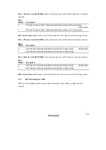
Страница 995: ...ion Date 1st Edition December 1997 5th Edition March 2002 Published by Business Planning Division Semiconductor Integrated Circuits Hitachi Ltd Edited by Technical Documentation Group Hitachi Kodaira Semiconductor Co Ltd Copyright Hitachi Ltd 1997 All rights reserved Printed in Japan ...

Отзывы: