481
17.2.2
Block Diagram
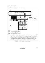
Figure 17.1 shows a block diagram of the flash memory.
Bus interface/controller
On-chip Flash memory
(128 kbytes)
Operating
mode
Internal data bus (upper 8 bits)
Internal data bus (lower 8 bits)
FWE pin
*
1
Mode pins
FLMCR
EBR
RAMCR
FLMSR
H'00000
H'00002
H'00001
H'00003
H'1FFFE
H'1FFFF
even address odd address
Legend:
FLMCR : Flash memory control register
*
2
EBR
: Erase block register
*
2
RAMCR : RAM control register
*
2
FLMSR : Flash memory status register
*
2
H'1FFFC
H'1FFFD
Notes:
*
1 Functions as the FWE pin in the versions with on-chip flash memory, and as the
RESO
pin in the versions with on-chip mask ROM.
*
2 The registers that control the flash memory (FLMCR, EBR, RAMCR, and FLMSR) are
used only in the versions with on-chip flash memory. They are not provided in the
versions with on-chip mask ROM. Reading the corresponding addresses in a mask
ROM version will always return 1s, and writes to these addresses are disabled.
Figure 17.1 Block Diagram of Flash Memory
Содержание H8/3060
Страница 10: ......
Страница 16: ......
Страница 114: ...66 ...
Страница 132: ...84 ...
Страница 144: ...96 ...
Страница 170: ...122 ...
Страница 212: ...164 ...
Страница 268: ...220 ...
Страница 332: ...284 ...
Страница 396: ...348 ...
Страница 494: ...446 ...
Страница 698: ...650 ...
Страница 729: ...681 H8 3062F ZTAT or H8 3062F ZTAT R mask version Ports 1 2 5 LED 600 Ω Figure 22 5 Sample LED Circuit ...
Страница 748: ...700 H8 3064F ZTAT B mask version Ports 1 2 5 LED 600 Ω Figure 22 8 Sample LED Circuit ...
Страница 777: ...729 H8 3062F ZTAT B mask version Ports 1 2 5 LED 600 Ω Figure 22 14 Sample LED Circuit ...
Страница 810: ...762 ...
Страница 994: ...946 ...

