64
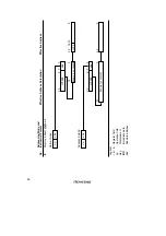
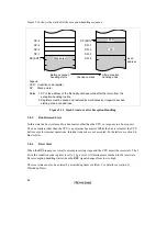
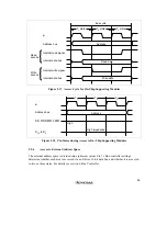
T state
Bus cycle
Internal address bus
Internal read signal
Internal data bus
(read access)
Internal write signal
Internal data bus
(write access)
φ
1
T state
2
Read data
Address
Write data
Figure 2.15 On-Chip Memory Access Cycle
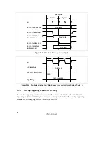
T
, , ,
AS
φ
1
T
2
Address bus
D to D
15
0
RD HWR LWR
High
Address
High impedance
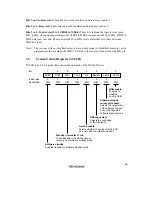
Figure 2.16 Pin States during On-Chip Memory Access (Address Update Mode 1)
2.9.3
On-Chip Supporting Module Access Timing
The on-chip supporting modules are accessed in three states. The data bus is 8 or 16 bits wide,
depending on the internal I/O register being accessed. Figure 2.17 shows the on-chip supporting
module access timing. Figure 2.18 indicates the pin states.
Содержание H8/3060
Страница 10: ......
Страница 16: ......
Страница 114: ...66 ...
Страница 132: ...84 ...
Страница 144: ...96 ...
Страница 170: ...122 ...
Страница 212: ...164 ...
Страница 268: ...220 ...
Страница 332: ...284 ...
Страница 396: ...348 ...
Страница 494: ...446 ...
Страница 698: ...650 ...
Страница 729: ...681 H8 3062F ZTAT or H8 3062F ZTAT R mask version Ports 1 2 5 LED 600 Ω Figure 22 5 Sample LED Circuit ...
Страница 748: ...700 H8 3064F ZTAT B mask version Ports 1 2 5 LED 600 Ω Figure 22 8 Sample LED Circuit ...
Страница 777: ...729 H8 3062F ZTAT B mask version Ports 1 2 5 LED 600 Ω Figure 22 14 Sample LED Circuit ...
Страница 810: ...762 ...
Страница 994: ...946 ...


