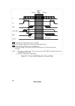
609
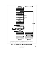
End of erasing
Start
Set SWE bit in FLMCR1
Set ESU bit in FLMCR1
Set E bit in FLMCR1
Wait (t
sswe
)
µ
s
Wait (t
sesu
)
µ
s
n = 1
Set EBR
Enable WDT
*
3,
*
4
*
5
*
5
*
5
*
5
*
5
*
5
*
5
*
5
*
5
*
5
*
5
*
5
Wait (t
se
) ms
Wait (t
ce
)
µ
s
Wait (t
cesu
)
µ
s
Wait (t
sev
)
µ
s
Set block start address as verify address
Wait (t
sevr
)
µ
s
*
2
Wait (t
cev
)
µ
s
Start of erase
Clear E bit in FLMCR1
Clear ESU bit in FLMCR1
Set EV bit in FLMCR1
H'FF dummy write to verify address
Read verify data
Clear EV bit in FLMCR1
Wait (t
cev
)
µ
s
Clear EV bit in FLMCR1
Clear SWE bit in FLMCR1
Disable WDT
Erase halted
*
1
Verify data = all 1s?
Last address of block?
Erase failure
Clear SWE bit in FLMCR1
n
≥
N?
No
No
No
Yes
Yes
Yes
n
←
n + 1
Increment
address
Wait (t
cswe
)
µ
s
Wait (t
cswe
)
µ
s
Notes:
*
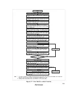
1 Prewriting (setting erase block data to all 0s) is not necessary.
*
2 Verify data is read in 16-bit (word) units.
*
3 Make only a single-bit specification in the erase block register (EBR). Two or more bits must not be set simultaneously.
*
4 Erasing is performed in block units. To erase multiple blocks, each block must be erased in turn.
*
5 The wait times and the value of N are shown in section 22.5.6, Flash Memory Characteristics.
Perform erasing in block units.
Figure 19.12 Erase/Erase-Verify Flowchart (Single-Block Erasing)
Содержание H8/3060
Страница 10: ......
Страница 16: ......
Страница 114: ...66 ...
Страница 132: ...84 ...
Страница 144: ...96 ...
Страница 170: ...122 ...
Страница 212: ...164 ...
Страница 268: ...220 ...
Страница 332: ...284 ...
Страница 396: ...348 ...
Страница 494: ...446 ...
Страница 698: ...650 ...
Страница 729: ...681 H8 3062F ZTAT or H8 3062F ZTAT R mask version Ports 1 2 5 LED 600 Ω Figure 22 5 Sample LED Circuit ...
Страница 748: ...700 H8 3064F ZTAT B mask version Ports 1 2 5 LED 600 Ω Figure 22 8 Sample LED Circuit ...
Страница 777: ...729 H8 3062F ZTAT B mask version Ports 1 2 5 LED 600 Ω Figure 22 14 Sample LED Circuit ...
Страница 810: ...762 ...
Страница 994: ...946 ...

