598
Notes on Use of Boot Mode:
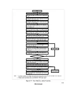
1. When the H8/3062F-ZTAT B-mask version chip comes out of reset in boot mode, it measures
the low period of the input at the SCI’s RxD
1
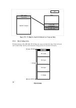
pin. The reset should end with RxD
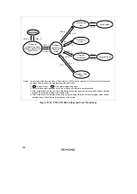
1
high. After
the reset ends, it takes about 100 states for the chip to get ready to measure the low period of
the RxD
1
input.
2. In boot mode, if any data has been programmed into the flash memory (if all data is not 1), all
flash memory blocks are erased. Boot mode is for use when user program mode is unavailable,
such as the first time on-board programming is performed, or if the program activated in user
program mode is accidentally erased.
3. Interrupts cannot be used while the flash memory is being programmed or erased.
4. The RxD
1
and TxD
1
lines should be pulled up on the board.
5. Before branching to the user program the H8/3062F-ZTAT B-mask version terminates transmit
and receive operations by the on-chip SCI (channel 1) (by clearing the RE and TE bits to 0 in
the serial control register (SCR)), but the adjusted bit rate value remains set in the bit rate
register (BRR). The transmit data output pin, TxD
1
, goes to the high-level output state
(P9
1
DDR = 1 in P9DDR, P9
1
DR = 1 in P9DR).
The contents of the CPU’s internal general registers are undefined at this time, so these
registers must be initialized immediately after branching to the user program. In particular,
since the stack pointer (SP) is used implicitly in subroutine calls, etc., a stack area must be
specified for use by the user program.
The initial values of other on-chip registers are not changed.
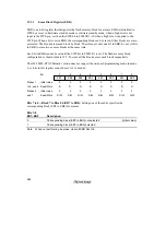
6. Boot mode can be entered by setting pins MD
0
to MD
2
and FWE in accordance with the mode
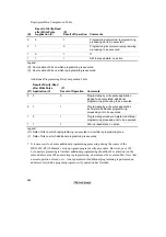
setting conditions shown in table 19.6, and then executing a reset-start.
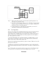
a. When switching from boot mode to normal mode, the boot mode state within the chip must
first be cleared by reset input via the
RES
pin*
1
. The
RES
pin must be held low for at least
20 system clock cycles*
2
.
b. Do not change the input levels of the mode pins (MD
2
to MD
0
) or the FWE pin in boot
mode. To change the mode, the
RES
pin must first be driven low to set the reset state.
Also, if a watchdog timer reset occurs in the boot mode state, the MCU’s internal state will
not be cleared, and the on-chip boot program will be restarted regardless of the mode pin
states.
c. The FWE pin must not be driven low while the boot program is running or flash memory is
being programmed or erased*
3
.
7. If the mode pin input levels are changed (for example, from low to high) during a reset, the
state of ports with multiplexed address functions and bus control output signals (
CSn
,
AS
,
RD
,
LWR
,
HWR
) may also change according to the change in the MCU’s operating mode.
Therefore, care must be taken to make pin settings to prevent these pins from being used
directly as output signal pins during a reset, or to prevent collision with signals outside the
MCU.
Содержание H8/3060
Страница 10: ......
Страница 16: ......
Страница 114: ...66 ...
Страница 132: ...84 ...
Страница 144: ...96 ...
Страница 170: ...122 ...
Страница 212: ...164 ...
Страница 268: ...220 ...
Страница 332: ...284 ...
Страница 396: ...348 ...
Страница 494: ...446 ...
Страница 698: ...650 ...
Страница 729: ...681 H8 3062F ZTAT or H8 3062F ZTAT R mask version Ports 1 2 5 LED 600 Ω Figure 22 5 Sample LED Circuit ...
Страница 748: ...700 H8 3064F ZTAT B mask version Ports 1 2 5 LED 600 Ω Figure 22 8 Sample LED Circuit ...
Страница 777: ...729 H8 3062F ZTAT B mask version Ports 1 2 5 LED 600 Ω Figure 22 14 Sample LED Circuit ...
Страница 810: ...762 ...
Страница 994: ...946 ...

