453
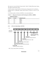
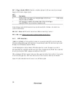
Bit 3—Clock Select (CKS): Selects the A/D conversion time. Clear the ADST bit to 0 before
switching the conversion time.
Bit 3
CKS
Description
0
Conversion time = 134 states (maximum)
(Initial value)
1
Conversion time = 70 states (maximum)
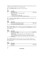
Bits 2 to 0—Channel Select 2 to 0 (CH2 to CH0): These bits and the SCAN bit select the analog
input channels. Clear the ADST bit to 0 before changing the channel selection.
Group
Selection
Channel Selection
Description
CH2
CH1
CH0
Single Mode
Scan Mode
0
0
0
AN
0
(Initial value)
AN
0
1
AN
1
AN
0
, AN
1
1
0
AN
2
AN
0
to AN
2
1
AN
3
AN
0
to AN
3
1
0
0
AN
4
AN
4
1
AN
5
AN
4
, AN
5
1
0
AN
6
AN
4
to AN
6
1
AN
7
AN
4
to AN
7
14.2.3
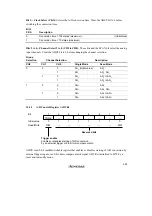
A/D Control Register (ADCR)
Bit
Initial value
Read/Write
7
TRGE
0
R/W
6
—
1
—
5
—
1
—
4
—
1
—
3
—
1
—
0
—
0
R/W
2
—
1
—
1
—
1
—
Trigger enable
Enables or disables starting of A/D conversion
by an external trigger or 8-bit timer compare match
Reserved bits
ADCR is an 8-bit readable/writable register that enables or disables starting of A/D conversion by
external trigger input or an 8-bit timer compare match signal. ADCR is initialized to H'7F by a
reset and in standby mode.
Содержание H8/3060
Страница 10: ......
Страница 16: ......
Страница 114: ...66 ...
Страница 132: ...84 ...
Страница 144: ...96 ...
Страница 170: ...122 ...
Страница 212: ...164 ...
Страница 268: ...220 ...
Страница 332: ...284 ...
Страница 396: ...348 ...
Страница 494: ...446 ...
Страница 698: ...650 ...
Страница 729: ...681 H8 3062F ZTAT or H8 3062F ZTAT R mask version Ports 1 2 5 LED 600 Ω Figure 22 5 Sample LED Circuit ...
Страница 748: ...700 H8 3064F ZTAT B mask version Ports 1 2 5 LED 600 Ω Figure 22 8 Sample LED Circuit ...
Страница 777: ...729 H8 3062F ZTAT B mask version Ports 1 2 5 LED 600 Ω Figure 22 14 Sample LED Circuit ...
Страница 810: ...762 ...
Страница 994: ...946 ...


