Geehy SEMICONDUCTOR APM32F405 Series Скачать руководство пользователя страница 169


www.geehy.com                                                                                                                                        Page  168


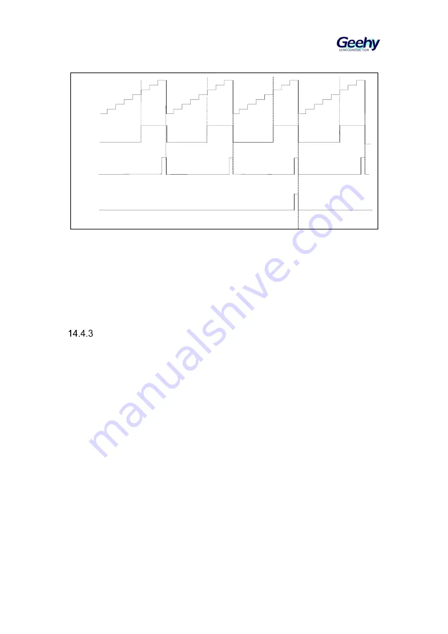
Figure 21 Timing Diagram when Setting REPCNT=2 in Count-up Mode 

CK_CNT

Counter 
overrun

Update 

event


Prescaler PSC 

The prescaler is 16 bits and programmable, and it can divide the clock 
frequency of the counter to any value between 1 and 65536 (controlled by 
TMRx_PSC register), and after frequency division, the clock will drive the 
counter CNT to count. The prescaler has a buffer, which can be changed during 
running. 


Input capture 

Input capture channel 

The advanced timer has four independent capture/compare channels, each of 
which is surrounded by a capture/compare register. 

In the input capture, the measured signal will enter from the external pin 
T1/2/3/4 of the timer, first pass through the edge detector and input filter, and 
then into the capture channel. Each capture channel has a corresponding 
capture register. When the capture occurs, the value of the counter CNT will be 
latched in the capture register CCx. Before entering the capture register, the 
signal will pass through the prescaler, which is used to set how many events to 
capture at a time. 

Input capture application 

Input capture is used to capture external events, and can give the time flag to 
indicate the occurrence time of the event and measure the pulse jump edge 
events (measure the frequency or pulse width), for example, if the selected 
edge appears on the input pin, the TMRx_CCx register will capture the current 
value of the counter and the CCxIFLG bit of the state register TMRx_STS will be 
set to 1; if CCxIEN=1, an interrupt will be generated. 

Содержание APM32F405 Series

Страница 1: ...www geehy com Page 0 User Manual APM32F405 415xG APM32F407 417xExG Arm Cortex M4 based 32 bit MCU Version V1 4...

Страница 2: ...ster address mapping 25 Register functional description 25 External Memory Controller EMMC 30 Full name and abbreviation description of terms 30 EMMC Overview 30 SMC Introduction 30 SMC Structure Bloc...

Страница 3: ...name and abbreviation description of terms 112 Introduction 112 Main characteristics 112 Interrupt and exception vector table 112 External Interrupt Event Controller EINT 120 Introduction 120 Main Ch...

Страница 4: ...mapping 180 Register functional description 181 General purpose timer TMR2 3 4 5 200 Introduction 200 Main characteristics 200 Structure block diagram 201 Functional description 201 Register address m...

Страница 5: ...terms 272 Introduction 272 Main characteristics 272 Structure block diagram 272 Functional description 273 Register address mapping 279 Register functional description 280 HASH processor HASH 296 Int...

Страница 6: ...nd abbreviation description of terms 357 Introduction 357 Main characteristics 358 SPI functional description 359 I2S functional description 370 Register address mapping 382 Register functional descri...

Страница 7: ...description 519 High speed OTG power and clock gating control register OTG_HS1_PCGCTRL 537 OTG_HS2 register address mapping 538 OTG_HS2 global register functional description 538 Ethernet 540 Introduc...

Страница 8: ...egister address mapping 646 Register functional description 646 CRYP 649 Introduction 649 Main characteristics 649 Interrupt 649 DMA 650 Register address mapping 650 Register functional description 65...

Страница 9: ...erb abbreviations to make a distinction The verbs can be EN Enable CFG Configure D Disable SET Setup and SEL Select The state register abbreviation is usually followed by FLG to make a difference The...

Страница 10: ...are can flip this bit only by writing 1 and writing 0 has no effect on this bit T Table 2 Functional Description and Full Name and Abbreviation of Terms of Commonly Used Registers Full name in English...

Страница 11: ...it RCM Power Management Unit PMU Backup Register BAKPR Nested Vector Interrupt Controller NVIC External Interrupt Event Controller EINT Direct Memory Access DMA Debug MCU DBG MCU General Purpose Input...

Страница 12: ...abbreviation Controller Area Network CAN Secure Digital Input and Output SDIO Universal Serial Bus Full Speed Device USBD Analog to Digital Converter ADC Digital to Analog Converter DAC Cyclic Redunda...

Страница 13: ...nal memory SRAM2 AHB1 bus and AHB1 APB bridge connected peripherals peripherals on AHB2 bus and EMMC The bus matrix provides a platform to support the master module to access the slave module The matr...

Страница 14: ...and the bus matrix The data are loaded stored in the memory through Ethernet DMA USB OTG HS DMA bus Connect the main interface of USB OTG HS DMA and the bus matrix The data are loaded stored in the me...

Страница 15: ...3 USART2 3 UART4 5 I2C1 2 3 TMR1 8 9 10 11 USART1 6 ADC1 2 3 SDIO SPI1 SYSCFG EINT T Sensor CAN1 2 DAC1 2 AHB1 I Code D Code GPIO A I CRC RCM Fast USB OTG Camera interface RNG D bus AHB2 CRYP Note 1 A...

Страница 16: ...ss of SRAM1 and SRAM2 is 0x2000 0000 and the main module can be accessoed by all AHB Core couple memory CCM The mapping address of CCM 64KB is 0x1000 0000 and it can only be accessed by CPU through D...

Страница 17: ...e system memory is 0x1FFF 0000 4 The starting address of SRAM is 0x2000 0000 5 The user can select the startup mode after reset by setting the state of BOOT 1 0 pin 6 BOOT pin should keep the user s r...

Страница 18: ...structure Contain main memory area and information block The capacity of main memory area is up to 1MB The information block is divided into system memory OTP area and option byte three areas The capa...

Страница 19: ...7 417xExG series products is related to the capacity of specific Flash see the Data Manual for the capacity of Flash of different models Flash memroy functional description Read Flash Flash has a pref...

Страница 20: ...EN bit of FMC_ACCTRL register D cache D cache is a data buffer memory The system accesses the data buffer area of Flash through D Bus to reduce the waiting time Access of D bus is prior to I bus The s...

Страница 21: ...ng it to avoid the loss of important data caused by misoperation Mass erase does not affect OTP sector or configuration sector Write main memory block Flash supports byte half word word and double wor...

Страница 22: ...Flash involves the data in D cache or I cache the data shall be written to the cache before it Interrupt An interrupt will occur in case of any of the following events End of operation End of erase wr...

Страница 23: ...bit to be cleared to zero Lock unlock FMC_OPTCTRL OPTLOCK can only be set to 1 so as to lock the option byte area Write the keywords 0x0819 2A3B and 0x4C5D 6E7F to the FMC_OPTKEY register and when the...

Страница 24: ...e operation for user configuration area Perform write operation for the locked OTP area Read protection In order to prevent untrusted code from reading Flash data you can choose to use the read protec...

Страница 25: ...emory JTAG SWV ETM and boundary scan is disabled The option byte is locked Note When the read protection level is set to 2 it cannot be degraded any more OTP The following table shows OTP structure Ta...

Страница 26: ...sh key register 0x04 FMC_OPTKEY Flash option key register 0x08 FMC_STS Flash state register 0x0C FMC_CTRL Flash control register 0x10 FMC_OPTCTRL Flash option control register 0x14 Register functional...

Страница 27: ...into this register Flash state register FMC_STS Offset address 0x0C Reset value 0x0000 0000 Field Name R W Description 0 OPRCMP RC_W1 Operation Complete This bit will be set to 1 when the operation fo...

Страница 28: ...g can be enabled 1 SERS R W Sector Erase When this bit is set to 1 sector erase can be enabled 2 MERS R W Mass Erase When this bit is set to 1 mass erase can be enabled 6 3 SNUM R W Sector Number This...

Страница 29: ...bit is set to 1 by the software the option byte can be operated and it can be cleared to zero when the BUSY bit is set to zero 3 2 BORLVL R W Brownout Reset Level When the power supply voltage is less...

Страница 30: ...www geehy com Page 29 Field Name R W Description 27 16 NWPROT R W Not Write Protect 0 Write protection isenabled 1 Write protection is disabled 31 28 Reserved...

Страница 31: ...X Width WID Flash Memory FM Access ACC Wait W Signal S Polarity POL Asynchronous ASYN Burst BURST Timing TIM Setup SET Hold HLD Empty E EMMC Overview EMMC includes SMC static memory controller and DMC...

Страница 32: ...roller Interrupt from SMC to NVIC SMC_NE 4 1 SMC_NL or NADV SMC_NBL 1 0 SMC_CLK SMC_A 25 0 SMC_D 15 0 SMC_NOE SMC_NWE SMC_NWAIT SMC_NCE 3 2 SMC_INT 3 2 SMC_INTR SMC_NCE4_1 SMC_NCE4_2 SMC_NIORD SMC_NIO...

Страница 33: ...ported 0x60000000 0x6FFFFFFF Memory block 1 4 64MB NOR PSRAM 0x70000000 0x7FFFFFFF Memory block 2 4 64MB NAND 0x80000000 0x8FFFFFFF Memory block 3 4 64MB NAND 0x90000000 0x9FFFFFFF Memory block 4 4 64...

Страница 34: ...Interface Signal SMC signal name Signal direction Function CLK Output Synchronous clock signal NE x Output Chip selection signal x 1 4 NOE Output Read enable signal NEW Output Write enable signal NWAI...

Страница 35: ...2 17 Clock division factor The ratio of memory access clock cycle CLK to AHB clock cycle Synchronous AHB clock cycle HCLK 2 16 Bus recovery time Duration of Bus recovery phase Asynchronous or synchro...

Страница 36: ...ading and writing to the memory Read Write data The operation address of the corresponding three step operation corresponds to the three blocks in the memory block To transmit a command to the memory...

Страница 37: ...p selection signal 1 NCE4_2 Output Chip selection signal 2 select 16 bit or 8 bit operation NOE Output Read enable signal NEW Output Write enable signal NWAIT Input PC card wait signal INTR Input PC c...

Страница 38: ...and 1 255 SMC register address mapping Table 26 SMC Register Address Mapping Register name Description Offset address SMC_CSCTRL1 4 SRAM NOR flash memory chip selection control register 1 4 8 x 1 x 1...

Страница 39: ...M 10 NORFlash default value after Bank1 reset Others Reserved 5 4 MDBWIDCFG R W Memory Data Bus Width Configure 00 8 bits 01 16 bits Others reserved 6 NORFMACCEN R W NORFlash Memory Access Enable 0 Di...

Страница 40: ...nchronous Transfers Enable This bit is used to enable SMC to use NWAIT signal during asynchronous protocol period 0 Disable 1 Enable 18 16 CRAMPSIZECFG R W CRAM Page Size Configure 000 There is no bur...

Страница 41: ...Phase Duration Configure These bits are used to configure the delay time on the bus after a read operation They are only applicable to NOR flash memory operation in bus multiplexing mode 0000 1 HCLK...

Страница 42: ...ock cycles Note In synchronous operation this parameter is meaningless and is always 1 memory clock cycle 7 4 ADDRHLDCFG R W Address Hold Time Configure Only apply to NOR flash memory operation in SRA...

Страница 43: ...cycles during the first burst access 1111 Data delay of 17 CLK clock cycles during the first burst access default value after reset This bit is invalid in asynchronous NOR Flash SRAM or ROM access mo...

Страница 44: ...evel 0000 1 HCLK cycle 0000 2 HCLK cycles 1111 16 HCLK cycles 16 13 A2RDCFG R W ALE To RE Delay Configure Configure the duration from ALE becomes low level to RE becomes low level 0000 1 HCLK cycle 00...

Страница 45: ...W Interrupt High Level Detection Enable 0 Disable 1 Enable 5 IFEDEN R W Interrupt Falling Edge Detection Enable 0 Disable 1 Enable 6 FEFLG R FIFO Empty Flag 0 Not empty 1 Empty 31 7 Reserved General...

Страница 46: ...1 HCLK cycle for write accesses 3 HCLK cycles for read accesses 0000 0010 2 HCLK cycles 1111 1110 254 HCLK cycles for write accesses 256 HCLK cycles for read accesses 1111 1111 Reserved 31 24 HIZx R...

Страница 47: ...ing the command 0000 0000 Reserved 0000 0001 1 HCLK cycle for write accesses 3 HCLK cycles for read accesses 0000 0010 2 HCLK cycles 1111 1110 254 HCLK cycles for write accesses 256 HCLK cycles for re...

Страница 48: ...nding the command 0000 0000 Reserved 0000 0001 1 HCLK cycle 0000 0010 2 HCLK cycles 1111 1111 255 HCLK cycles 31 24 HIZ R W I O x Databus Hiz Time Configure This bit takes HCLK as the clock cycle and...

Страница 49: ...ry controller AHB Off chip SDR SDRAM DMC functional description DMC external memory interface The signal with the prefix N means low effective signal Table 27 DMC Pins Signal Name Input Output Pin Fun...

Страница 50: ...ctional data D12 Input Output PD13 Bidirectional data D13 Input Output PD14 Bidirectional data D14 Input Output PD15 Bidirectional data D15 Input Output PG2 Bidirectional data BA Output PI11 Bank addr...

Страница 51: ...ister name Description Offset address DMC_CFG Configuration register 0x00 DMC_TIM0 Timing register 0 0x04 DMC_TIM1 Timing register 1 0x08 DMC_CTRL1 Control register 1 0x0C DMC_REF Refresh register 0x1...

Страница 52: ...Select CAS CASLSEL0 ECASLSEL1 2 00 1 clock cycle 01 2 clock cycles 10 3 clock cycles 11 4 clock cycles Others Reserved 5 2 RASMINTSEL R W RAS Minimum Time Select These bits are used to select the min...

Страница 53: ...M0_CASLSEL0 interpretation 31 27 EXSR1 R W Minimum interval time from exiting self refresh switch to activation command or auto refresh read command See TIM0_XSR0 interpretation Timing register 1 DMC_...

Страница 54: ...h mode 1 Refresh all rows after exiting self refresh mode 8 6 RDNUMCFG R W Configure Number Of Registers Inserted In Read Data Path 000 0 register 001 1 register 111 7 registers 9 MODESET R W Mode Set...

Страница 55: ...m clock is not reverse 1 The system clock is reverse 1 RDDEN R W RD Delay Function Enable 0 Enable 1 Disable 4 2 RDDCFG R W RD Clock Delay Configure 000 0 system clock 001 1 system clock 111 7 system...

Страница 56: ...29 SYSCFG Register Address Mapping Register name Description Offset address SYSCFG_MMSEL Memory mapping selection register 0x00 SYSCFG_PMCFG Peripheral mode configuration register 0x04 SYSCFG_EINTCFG1...

Страница 57: ...scription 22 0 Reserved 23 ENETSEL R W Ethernet PHY Interface Select Control the physical layer interface 0 MII interface 1 RMII PHY interface Note This bit shall be operated when ENET is reset and be...

Страница 58: ...ister 2 SYSCFG_EINTCFG2 Offset address 0x0C Reset value 0x0000 0000 These bits are controlled by software to be rewritten to select the external interrupt source of EINTx x 4 7 Field Name R W Descript...

Страница 59: ...source of EINTx x 12 15 Note that when the value of each bit of the register is 0x1000 this bit is reserved bit namely PI 15 12 is unused Field Name R W Description 3 0 EINT12 R W EINT12 Configure The...

Страница 60: ...www geehy com Page 59 Field Name R W Description 8 RDYFLG R Compensation Cell Ready Flag 0 Not ready 1 Ready 31 9 Reserved...

Страница 61: ...LSICLK Phase Locked Loop PLL Main clock output MCO Calibrate CAL Trim TRM Clock Security System CSS Non Maskable Interrupt NMI Reset management unit RMU The reset is divided into three forms namely s...

Страница 62: ...power management may reset in two cases one is when entering the standby mode and the other is when entering the stop mode In these two cases if RSTSTDBY in standby mode or RSTSTOP in stop mode in us...

Страница 63: ...ke up from standby mode A power reset will occur in case of any of the above events Power reset will reset all registers except that in backup domain Backup domain reset Backup domain reset reset sour...

Страница 64: ...ation of the two kinds of clock sources is shown in the figure below Figure 5 HSECLK LSECLK Clock Source Hardware Configuration OSC_OUT Hi Z External clock source Crystal ceramic resonator OSC_OUT OSC...

Страница 65: ...ol register RCM_CTRL clock control register HSERDYFLG bit in the clock control register RCM_CTRL clock control register is used to indicate whether the high speed external oscillator is stable After s...

Страница 66: ...each chip has been calibrated to 1 25 VDD VDDA 3 3V by the manufacturer before leaving the factory When the system is reset the value calibrated by the manufacturer will be loaded to RCM_CTRL register...

Страница 67: ...ter the stop or standby state The system clock directly or indirectly selects HSECLK as the clock source and a fault occurs to HSECLK When configuring PLL related coefficient ensure that it is not ena...

Страница 68: ...if APB2 prescaler 1 1 else 2 Analog ADC Prescaler 2 4 6 8 ADCCLK Analog HCLK PCLK1 FCLK 8 Cortex System Clock HSICLK LSECLK HSECLK PLL1CLK MCOSEL1 ETH PTP RTCSEL 1 0 SYSCLK 168MHz MAX MCO1 168MHz MAX...

Страница 69: ...the clock can be used by all ADC the clock frequency of digital circuit of ADC is equal to PCLK2 and ADC1 2 3 clocks can be enabled respectively through the corresponding bits of RCM_APB2CLKEN registe...

Страница 70: ...sponding multiplexing function the clock signal can be selected to be output to MCO pin by configuring MCOxSEL bit and MCOxPSC bit in RCM_CFG clock configuration register See the clock tree or registe...

Страница 71: ...Circuit Diagram TMR5 GPIO RTC_Wakeup_IT LSECLK LSICLK RMPSEL TI4 Channel 4 of TMR5 can select to connect one GPIO port or one MCU internal clock by configuring RMPSEL bit of TMR5_OPT register TMR11 ba...

Страница 72: ...ster 0x40 RCM_APB2CLKEN APB2 peripheral clock enble register 0x44 RCM_LPAHB1CLKEN AHB1 peripheral clock enable register in low power mode 0x50 RCM_LPAHB2CLKEN AHB2 peripheral clock enable register in...

Страница 73: ...HSICLK RC oscillator can be adjusted by this bit 15 8 HSICAL R High Speed Internal Clock Calibrate HSICLK has been calibrated to 16MHz 1 when the product leaves the factory When the system is started...

Страница 74: ...PLL2 is disabled 1 PLL2 is enabled 27 PLL2RDYFLG R PLL2 Clock Ready Flag PLL2 is set to 1 by hardware after it is locked 0 PLL2 is unlocked 1 PLL2 is locked 31 28 Reserved PLL1 configuration register...

Страница 75: ...eserved 22 PLLCLKS R W PLL Clock Source This bit can be set or cleared by software and be used to select the clock source of PLL1 and PLL2 0 HSICLK is used as clock source 1 HSECLK is used as clock so...

Страница 76: ...0 SYSCLK two divided frequency 1001 SYSCLK four divided frequency 1010 SYSCLK eight divided frequency 1011 SYSCLK 16 divided frequency 1100 SYSCLK 64 divided frequency 1101 SYSCLK 128 divided frequenc...

Страница 77: ...11111 HSECLK31 frequency division Note This bit must be configured before RTC selects HSECLK as the clock source 22 21 MCO1SEL R W Main Clock Output1 Select Set or cleared by software 00 HSICLK is ou...

Страница 78: ...y interrupt occurred 2 HSIRDYFLG R HSICLK Ready Interrupt Flag When HSICLK is stable and HSIRDYEN bit is set to 1 this bit will be set to 1 by hardware when HSIRDYCLR is set to 1 by software this bit...

Страница 79: ...terrupt 0 Disable 1 Enable 10 HSIRDYEN R W HSICLK Ready Interrupt Enable Enable the internal 8MHz RC oscillator ready interrupt 0 Disable 1 Enable 11 HSERDYEN R W HSCLKE Ready Interrupt Enable Enable...

Страница 80: ...d 23 CSSCLR W Clock Security System Interrupt Clear Clear the security system interrupt flag bit CSSFLG 0 No effect 1 Clear 31 24 Reserved AHB1 peripheral reset register RCM_AHB1RST Offset address 0x1...

Страница 81: ...0 No effect 1 Reset 22 DMA2RST R W DMA2 Reset 0 No effect 1 Reset ADC 24 23 Reserved 25 ETHRST R W ETH Reset 0 No effect 1 Reset 28 26 Reserved 29 OTGHS1RST R W OTGHS1 Reset 0 No effect 1 Reset 31 30...

Страница 82: ...l reset register RCM_AHB3RST Offset address 0x18 Reset value 0x0000 0000 Access Access in the form of word half word and byte without wait cycle Field Name R W Description 0 EMMCRST R W EMMC Reset 0 N...

Страница 83: ...2 Reset 0 No effect 1 Reset 7 TMR13RST R W TMR13 Reset 0 No effect 1 Reset 8 TMR14RST R W TMR14 Reset 0 No effect 1 Reset 10 9 Reserved 11 WWDTRST R W WWDT Reset 0 No effect 1 Reset 13 12 Reserved 14...

Страница 84: ...W CAN2 Reset 0 No effect 1 Reset 27 Reserved 28 PWRRST R W Power Interface Reset 0 No effect 1 Reset 29 DACRST R W DAC Interface Reset 0 No effect 1 Reset 31 30 Reserved APB2 peripheral reset registe...

Страница 85: ...R W SPI1 Reset 0 No effect 1 Reset 13 Reserved 14 SYSCFGRST R W SYSCFG Module Reset 0 No effect 1 Reset 15 Reserved 16 TMR9RST R W TMR9 Reset 0 No effect 1 Reset 17 TMR10RST R W TMR10 Reset 0 No effe...

Страница 86: ...PGEN R W GPIOG Clock Enable 0 Disable 1 Enable 7 PHEN R W GPIOH Clock Enable 0 Disable 1 Enable 8 PIEN R W GPIOI Clock Enable 0 Disable 1 Enable 11 9 Reserved 12 CRCEN R W CRC Clock Enable 0 Disable 1...

Страница 87: ...IEN R W OTG_HS1 ULPI Clock Enable 0 Disable 1 Enable 31 Reserved AHB2 peripheral clock enable register RCM_AHB2CLKEN Offset address 0x34 Reset value 0x0000 0000 Access Access in the form of word half...

Страница 88: ...k Enable 0 Disable 1 Enable 31 1 Reserved APB1 peripheral clock enable register RCM_APB1CLKEN Offset address 0x40 Reset value 0x0000 0000 Access Access in the form of word half word and byte without w...

Страница 89: ...I2EN R W SPI2 Clock Enable 0 Disable 1 Enable 15 SPI3EN R W SPI3 Clock Enable 0 Disable 1 Enable 16 Reserved 17 USART2EN R W USART2 Clock Enable 0 Disable 1 Enable 18 USART3EN R W USART3 Clock Enable...

Страница 90: ...fset address 0x44 Reset value 0x0000 0000 Access Access in the form of word half word and byte without wait cycle All bits can be reset or cleared by software Field Name R W Description 0 TMR1EN R W T...

Страница 91: ...TMR10 Clock Enable 0 Disable 1 Enable 18 TMR11EN R W TMR11 Clock Enable 0 Disable 1 Enable 31 19 Reserved AHB1 peripheral clock enable register in low power mode RCM_LPAHB1CLKEN Offset address 0x50 Re...

Страница 92: ...le 1 Enable 8 PIEN R W GPIOI Clock Enable 0 Disable 1 Enable 11 9 Reserved 12 CRCEN R W CRC Clock Enable 0 Disable 1 Enable 14 13 Reserved 15 FMCEN R W FMC Clock Enable 0 Disable 1 Enable 16 SRAM1EN R...

Страница 93: ...HSULPIEN R W OTG_HS1 ULPI Clock Enable 0 Disable 1 Enable 31 Reserved AHB2 peripheral clock enable register in low power mode RCM_LPAHB2CLKEN Offset address 0x54 Reset value 0x0000 00F1 Access Access...

Страница 94: ...ait cycle The function of this register is to enable the peripheral clock of AHB3 in low power sleep mode Field Name R W Description 0 EMMCEN R W EMMC Clock Enable 0 Disable 1 Enable 31 1 Reserved APB...

Страница 95: ...0 Disable 1 Enable 7 TMR13EN R W TMR13 Clock Enable 0 Disable 1 Enable 8 TMR14EN R W TMR14 Clock Enable 0 Disable 1 Enable 10 9 Reserved 11 WWDTEN R W WWDT Clock Enable 0 Disable 1 Enable 13 12 Reser...

Страница 96: ...28 PMUEN R W PMU Clock Enable 0 Disable 1 Enable 29 DACEN R W DAC Interface Clock Enable 0 Disable 1 Enable 31 30 Reserved APB2 peripheral clock enable register in low power mode RCM_LPAPB2CLKEN Offs...

Страница 97: ...DIOEN R W SDIO Clock Enable 0 Disable 1 Enable 12 SPI1EN R W SPI1 Clock Enable 0 Disable 1 Enable 13 Reserved 14 SYSCFGEN R W SYSCFG Module Clock Enable 0 Disable 1 Enable 15 Reserved 16 TMR9EN R W TM...

Страница 98: ...T bit to reset the RTC domain and then select the RTC clock source It is impossible to directly configure the register to modify 00 No clock 01 LSECLK is used as RTC clock 10 LSICLK is used as RTC clo...

Страница 99: ...Flag It is set by hardware when pin reset occurs otherwise it is cleared by setting RSTFLGCLR 0 Reset does did not occur 1 Reset occurred 27 PODRSTFLG R POR PDR Reset Flag Set to 1 by hardware cleared...

Страница 100: ...n period 27 13 STEP R W Incrementation Step Set to 1 or cleared by software Configure the input of modulation amplitude 29 28 Reserved 30 SSSEL R W Spread Spectrum Select It is set or cleared by softw...

Страница 101: ...served 30 28 PLL2C R W Division Factor This bit can be set or cleared by software and this variable can be controlled to change the clock frequency provided to I2S This bit can be set only when PLL2 i...

Страница 102: ...Power Management Unit PMU Power On Reset POR Power Down Reset PDR Brown out Reset BOR Power Voltage Detector PVD Introduction The power supply is the basis for stable operation of a system The working...

Страница 103: ...M AHB digital peripheral APB digital peripheral LSECLK crystal resonator Backup register Backup SRAM RTC Wake up logic Reset controller VCAP_1 VCAP_2 GPIO PDR_ON BYPASS_REG Functional description Powe...

Страница 104: ...cific power pins are as follows VDDA Power pin of ADC VSSA Independent power ground pin VREF VREF ADC reference voltage pin 1 3V power domain The core Flash SRAM and digital peripherals are powered by...

Страница 105: ...ower than the threshold voltage VBOR the chip will automatically remain in reset state and VBOR can be configured through option byte The followings are 4 thresholds of VBOR VBOR0 BOR is turned off an...

Страница 106: ...usage of PVD is as follows Set the PVDEN bit of the configuration register PMU_CTRL to 1 to enable PVD Select the voltage threshold of PVD for the PLSEL 2 0 bit of the configuration register PMU_CTRL...

Страница 107: ...ode and data storage of each low power mode are different the lower the power consumption is the longer the wake up time is the less the wake up mode is the less the data saved are after wake up users...

Страница 108: ...TC timestamp event RTC tamper event external reset on NRST pin and IWDT reset Off Sleep mode The characteristics of sleep mode are shown in the table below Table 39 Characteristics of Sleep Mode Chara...

Страница 109: ...the data in the core register and memory before stop will be saved Wake up delay HSICLK oscillator wake up time voltage regulator wake up time from low power mode After wake up If the system is woken...

Страница 110: ...s 0x00 Reset value 0x0000 0000 cleared when waking up from standby mode Field Name R W Description 0 LPDSCFG R W Low Power Deepsleep Configure Configure the working state of the voltage regulator in s...

Страница 111: ...it requires extra APB cycle to read this register Field Name R W Description 0 WUEFLG R Wakeup Event Flag This bit is set by hardware indicating whether wake up event or RTC alarm wake up event RTC t...

Страница 112: ...KUP Pin Configure When WKUP is used as a normal I O the event on WKUP pin cannot wake up the CPU in standby mode it can wake up CPU only when it is not used as a normal I O 0 Configure normal I O 1 Ca...

Страница 113: ...structions about NVIC Main characteristics 85 maskable interrupt channels excluding 16 Arm Cortex M4 interrupt lines 8 programmable priority levels use 3 bit interrupt priority level Low delay excepti...

Страница 114: ...an be set 0x0000_0058 EINT Line 0 interrupt EINT1 7 Can be set 0x0000_005C EINT Line 1 interrupt EINT2 8 Can be set 0x0000_0060 EINT Line 2 interrupt EINT3 9 Can be set 0x0000_0064 EINT Line 3 interru...

Страница 115: ...error interrupt I2C2_EV 33 Can be set 0x0000_00C4 I2C2 event interrupt I2C2_ER 34 Can be set 0x0000_00C8 I2C2 error interrupt SPI1 35 Can be set 0x0000_00CC SPI1 interrupt SPI2 36 Can be set 0x0000_0...

Страница 116: ...000_0138 Ethernet wake up interrupt through EINT line CAN2_TX 63 Can be set 0x0000_013C CAN2 transmitting interrupt CAN2_RX0 64 Can be set 0x0000_0140 CAN2 receiving 0 interrupt CAN2_RX1 65 Can be set...

Страница 117: ...system service revoking Debug Monitor Can be set 0x0000_0030 Debug monitor 0x0000_0034 Reserved PendSV Can be set 0x0000_0038 Pending system service request SysTick Can be set 0x0000_003C System tick...

Страница 118: ...0x0000_0094 CAN1 receiving 1 interrupt CAN1_SCE 22 Can be set 0x0000_0098 CAN1 SCE interrupt EINT9_5 23 Can be set 0x0000_009C EINT line 9 5 interrupt TMR1_BRK_TMR9 24 Can be set 0x0000_00A0 TMR1 brak...

Страница 119: ...n be set 0x0000_0104 SDIO interrupt TMR5 50 Can be set 0x0000_0108 TMR5 interrupt SPI3 51 Can be set 0x0000_010C SPI3 interrupt UART4 52 Can be set 0x0000_0110 UART4 interrupt UART5 53 Can be set 0x00...

Страница 120: ...0x0000_0160 I2C3 event interrupt I2C3_ER 73 Can be set 0x0000_0164 I2C3 error interrupt OTG_HS1_EP1_O UT 74 Can be set 0x0000_0168 OTG_HS1 endpoint 1 output interrupt OTG_HS1_EP1_IN 75 Can be set 0x00...

Страница 121: ...ed by hardware The external events output pulse through events such as GPIO while the internal events trigger another TMR to work for example through update event of one TMR Main Characteristics Suppo...

Страница 122: ...not be set to 1 External software interrupt Software interrupt register 1 Allow interrupt request and enable the corresponding peripheral interrupt line enable in NVIC 2 Write 1 to the software interr...

Страница 123: ...interrupt handler function Enable SEVONPEND bit in the system controller of the core and execute WFE instruction to make the core enter sleep mode Generate an interrupt to wake up the core when the c...

Страница 124: ...er address mapping Table 48 EINT Register Address Mapping Register name Description Offset address EINT_IMASK Interrupt mask register 0x00 EINT_EMASK Event mask register 0x04 EINT_RTEN Enable the risi...

Страница 125: ...e recognized and the set pending bit will not be set in the same interrupt line the rising edge trigger and falling edge trigger can be set at the same time Enable the falling edge trigger register EI...

Страница 126: ...terrupt event request an interrupt event will be generated 0 No effect 1 Software generates an interrupt event 31 23 Reserved Interrupt pending register EINT_IPEND Offset address 0x14 Reset value 0xXX...

Страница 127: ...s Dual AHB main interfaces one is memory interface and the other is peripheral interface There are three data transmission modes peripheral to memory memory to peripheral memory to memory Each data st...

Страница 128: ...tion DMA transmission error DMA FIFO error and direct mode error The logic of the five event flags may become a separate interrupt request and they all support software trigger When multiple periphera...

Страница 129: ...TX I2C1_TX Channel 2 TMR4_CH1 I2S3_EXT_ RX TMR4_CH2 I2S2_EXT_TX I2S3_EXT_TX TMR4_UP TMR4_CH3 Channel 3 I2S3_EXT_RX TMR2_UP TMR2_CH3 I2C3_RX I2S2_EXT_ RX I2C3_TX TMR2_CH1 TMR2_CH2 TMR2_CH4 TMR2_UP TMR2...

Страница 130: ...MR8_CH2 TMR8_CH3 ADC1 TMR1_CH1 TMR1_CH2 TMR1_CH3 Channel 1 DCI ADC2 ADC2 DCI Channel 2 ADC3 ADC3 CRYP_OUT CRYP_IN HASH_IN Channel 3 SPI1_RX SPI1_RX SPI1_TX SPI1_TX Channel 4 USART1_RX SDIO USART1_RX S...

Страница 131: ...mode and memory to memory transmission mode The second is FIFO mode in which FIFO threshold is configured first and when the data storage reaches the threshold FIFO content will be transmitted to the...

Страница 132: ...register and it can be configured as single transmission incremental burst transmission of 4 ticks incremental burst transmission of 8 ticks and incremental burst transmission of 16 ticks This increme...

Страница 133: ...DMA acesses DMA_M1ADDR CTARG bit of DMA_SCFG register will be set to 1 and can write or read data to DMA_M0ADDR register at the same time This mode does not support memory to memory transmission Strea...

Страница 134: ...0x00 DMA_HINTSTS DMA high interrupt state register 0x04 DMA_LIFCLR DMA low interrupt flag clear register 0x08 DMA_HIFCLR DMA high interrupt flag clear register 0x0C DMA_SCFG DMA data stream x configu...

Страница 135: ...et to 1 by hardware write 1 and set to 0 by software on the corresponding bit of DMA_LIFCLR register 0 No half transmission event 1 Half transmission event is generated 27 21 11 5 TXCIFLGx R Stream x...

Страница 136: ...Reserved DMA low interrupt flag clear register DMA_LIFCLR Offset address 0x08 Reset value 0x0000 0000 Field Name R W Description 22 16 6 0 CFEIFLGx W Stream x Clear FIFO Error Interrupt Flag x 0 3 0 I...

Страница 137: ...onding HTXIFLGx flag in DMA_HINTSTS register is cleared to 0 27 21 11 5 CTXCIFLGx W Stream x Clear Transfer Complete Interrupt Flag x 4 7 0 Invalid 1 The corresponding TXCIFLGx flag in DMA_HINTSTS reg...

Страница 138: ...nable If the peripheral is set as the stream controller and the data stream is enabled this bit will be automatically forced to 0 by hardware If DMA transmission is ended switch the target memory area...

Страница 139: ...e 0 Do not switch the buffer when the transmission ends 1 Switch the target memory when DMA transmission ends This bit can be written only when EN bit is 0 19 CTARG R W Current Target only in double b...

Страница 140: ...egister will decrease This register is 0 after completion of transmission and the initial value will be automatically reloaded in any of the following circumstances 1 Configure the data stream in circ...

Страница 141: ...tream x xFIFO control register DMA_FCTRL x 0 7 Offset address 0x24 0x18 data stream number Reset value 0x0000 0000 Field Name R W Description 1 0 FTHSEL R W FIFO Threshold Select 00 1 4 of FIFO capaci...

Страница 142: ...www geehy com Page 141 Field Name R W Description 7 FEIEN R W FIFO Error Interrupt Enable 0 Disable 1 Enable 31 8 Reserved...

Страница 143: ...al state of the core and the external state of the system and after the query is completed the core and peripheral operation can be restored to continue to execute the program Two debug interfaces are...

Страница 144: ...entation of production of bus line programmer Table 55 Pin Function Configuration SWJ CFG 2 0 Configured as dedicated pin for debugging I O port assignment of SWJ interface PA13 JTMS SWDIO PA14 JTCK S...

Страница 145: ...in 4KB ROM table in which the internal PPB bus address is 0xE0042000 Register address mapping Table 56 Register Address Mapping Register name Description Address DBGMCU_IDCODE Device ID register 0xE00...

Страница 146: ...by HSICLK 2 STANDBY_CLK_STS R W Configure clock status when MCU is debugged in standby mode 0 FCLK OFF HCLK OFF 1 FCLK ON HCLK ON provided by HSICLK 4 3 Reserved 5 TRACE_IOEN R W Trace Debug Pin Enab...

Страница 147: ...s to work when the core stops work 0 Continue to work 1 Stop working 4 TMR6_STS R W Configure Timer6 Work Status When Core is in Halted Whether TMR6 counter continues to work when the core stops work...

Страница 148: ...work when the core stops work 0 Work normally 1 Freeze the timeout mode of SMBUS 22 I2C2_SMBUS _TIMEOUT_S TS R W Configure I2C2_SMBUS_TIMEOUT Work Status When Core is in Halted Whether I2C2_SMBUS_TIM...

Страница 149: ...ork when the core stops work 0 Continue to work 1 Stop working 1 TMR8_STS R W ConfigureTimer8 Work Status When Core is in Halted Whether TMR8 continues to work when the core stops work 0 Continue to w...

Страница 150: ...s GPIO port can configure the following functions through 32 bit configuration register GPIOx_CFGLOW GPIOx_CFGHIG and two 32 bit data registers GPIOx_IDATA GPIOx_ODATA Input mode Analog input Floating...

Страница 151: ...nction through software All GPIO interfaces have external interrupt capability IO status during reset and just after reset If the multiplexing function is not enabled during and after GPIO reset the I...

Страница 152: ...down when connecting the equipment it is determined by the external input level and load impedance Analog input mode In analog input mode Disable output buffer The input of Schmitt trigger is disabled...

Страница 153: ...ead write Multiplexing function output From on chip peripheral Push pull open drain disable P MOS N MOS Write VDDIOx VSS I O pin PULL UP PULL DOWN Multiplexing mode In multiplexing mode it can be set...

Страница 154: ...ation can be realized GPIO locking function Locking function can be used in power driver module The locking mechanism of GPIO can protect the configuration of I O port I O configuration can be locked...

Страница 155: ...ultiplexing function mode 11 Analog mode Port output mode register GPIOx_OMODE x A I Offset address 0x04 Reset value 0x0000 0000 Field Name R W Description 15 0 OMODEy R W PortxPin y Output Mode Confi...

Страница 156: ...up Pull down Configure y 0 15 These bits are written by software to configure pull up pull down of the port bit 00 Pull up Pull down is disabled 01 Pull up 10 Pull down 11 Reset GPIO port input data...

Страница 157: ...O from being modified by mistake during the running of the program If the GPIO configuration is modified again it can be modified only after the system is reset When configuring GPIO locking function...

Страница 158: ...ame R W Description 31 0 ALFSELy R W Port x Pin y Alternate Function Select y 0 7 These bits can be read by software to configure the multiplexing function of the port ALFSELy selection 0000 AF0 0001...

Страница 159: ...geehy com Page 158 Field Name R W Description 0011 AF3 0100 AF4 0101 AF5 0110 AF6 0111 AF7 1000 Reserved 1001 Reserved 1010 Reserved 1011 Reserved 1100 Reserved 1101 Reserved 1111 Reserved 1110 Reser...

Страница 160: ...compare function braking and complementary output function and is a 16 bit timer that can count up down The function of general purpose timer is simpler than that of advanced timer The main differenc...

Страница 161: ...ne Single pulse mode Yes Yes Yes Yes None Forced output mode Yes Yes Yes Yes None Dead time insertion Yes None None None None Timer term Table 61 Definitions and Terms of Pins Name Description TMRx_ET...

Страница 162: ...1F Timer input filter TI1_ED Timer input edge detection TIxFPx TI1FP1 Timer input filter polarity ICx IC1 Input capture ICxPS IC1PS Input capture prescaler TRC Trigger capture BRK Braking signal OCx O...

Страница 163: ...Prescaler 16 bit programmable prescaler Repeat counter 16 bit repeat counter Auto reloading function Clock source selection Internal clock External input External trigger Internal trigger Input captur...

Страница 164: ...0 ITR1 ITR2 ITR3 ITR ETRF TRGI TI1FP1 TI2FP2 TI1FP1 TI2FP2 TI1F_ED TRC TRC ICx ICx ICxPS ICxPS DTS OC3REF Output contro DTS OCxREF Output control Internal clock CK_INT Polarity selection BRK Output co...

Страница 165: ...r timers At this time the clock source has no filtering and the synchronization or cascading between timers can be realized The master mode timer can reset start stop or provide clock for the slave mo...

Страница 166: ...Factor is 1 or 2 in Count up Mode Figure 18 Timing Diagram when Division Factor is 1 or 2 in Count up Mode CNT_EN CK_CNT 21 22 23 24 25 26 27 00 01 02 03 04 Counter register Counter overrun Update eve...

Страница 167: ...hen Division Factor is 1 or 2 in Count down Mode CNT_EN CK_CNT 06 05 04 03 02 01 00 26 25 24 23 22 Counter register Counter overrun Update event CK_PSC PSC 1 CK_CNT 21 20 0002 0001 0000 0026 0025 0024...

Страница 168: ...le in the advanced timer because of the existence of the repeat counter when an overrun unerrrun event occurs to the advanced timer the update event will be generated only when the value of the repeat...

Страница 169: ...in T1 2 3 4 of the timer first pass through the edge detector and input filter and then into the capture channel Each capture channel has a corresponding capture register When the capture occurs the v...

Страница 170: ...MRx_CCMx register and can control the waveform of output signal in output compare mode Output compare application In the output compare mode the position polarity frequency and time of the pulse gener...

Страница 171: ...e Timing Diagram CCx AUTORLD OCXREF Figure 24 PWM1 Center aligned Mode Timing Diagram AUTORLD CCx OCXREF In PWM mode 2 if the value of the counter CNT is less than that of the compare register CCx the...

Страница 172: ...e Timing Diagram CCx AUTORLD OCxREF PWM input mode PWM input mode is a particular case of input capture In PWM input mode as only TI1FP1 and TI1FP2 are connected to the slave mode controller input can...

Страница 173: ...iod The value is latched in TMRx_CC2 0003 0005 Single pulse mode The single pulse mode is a special case of timer compare output and is also a special case of PWM output mode Set SPMEN bit of TMRx_CTR...

Страница 174: ...MOEN 0 Idle mode MOEN 1 Run mode OCxOIS and OCxNOIS bits in TMRx_CTRL2 register OCxOIS 0 amd OCxNOIS 0 When idle MOEN 0 the output level after the dead time is 0 OCxOIS 1 amd OCxNOIS 1 When idle MOEN...

Страница 175: ...1 IMOS 0 CCxEN CCxNEN 1 CCxEN CCxNEN 0 CCxEN CCxNEN 1 CCxEN CCxNEN 0 Output disable first output 0 in the dead zone and after it is received by dead zone output the idle level OIS Output disable first...

Страница 176: ...annels The insertion dead time is used to generate complementary output signals to ensure that the two way complementary signals of channels will not be valid at the same time The dead time is set acc...

Страница 177: ...I2 by setting the CC1POL and CC2POL bits of TMRx_CCEN register Select to filter or not by setting the IC1F and IC2F bits of TMRx_CCM1 register The two input TI1 and TI2 can be used as the interface of...

Страница 178: ...d to convert the differential output of the encoder to digital signal to increase the immunity from noise interference Among the following examples IC1FP1 is mapped to TI1 IC2FP2 is mapped to TI2 Neit...

Страница 179: ...d generate a signal to update the register In the gated mode the enable of the counter depends on the high level of the selected input When the trigger input is high the clock of the counter will be s...

Страница 180: ...DMA request The timer can generate an interrupt when an event occurs during operation Update event counter overrun underrun counter initialization Trigger event counter start stop internal external tr...

Страница 181: ...lowing table all registers of the advanced timer are mapped to a 16 bit addressable address space Table 64 Advanced Timer Register Address Mapping Register name Description Offset address TMRx_CTRL1 C...

Страница 182: ...Enable 0 Disable 1 Enable When the timer is configured as external clock gated mode and encoder mode it is required to write 1 to the bit by software to start regular work when it is configured as th...

Страница 183: ...1 when counting down 10 Center aligned mode 2 the output compare interrupt flag bit of output channel is set to 1 when counting up 11 Cente aligned mode 3 the output compare interrupt flag bit of out...

Страница 184: ...001 Enable the counter enable signal of master mode timer is used for TRGO 010 Update the update event of master mode timer is used for TRGO 011 Compare pulses when the master mode timer captures com...

Страница 185: ...counts at the edge of TI1FP1 and TI2FP2 100 Reset mode the slave mode timer resets the counter after receiving the rising edge signal of TRGI and generates the signal to update the register 101 Gated...

Страница 186: ...MRxCLK frequency when ETR frequency is too high the ETRP frequency must be reduced through frequency division 00 The prescaler is disabled 01 ETR signal 2 divided frequency 10 ETR signal 4 divided fre...

Страница 187: ...hannel3 Interrupt Enable 0 Disable 1 Enable 4 CC4IEN R W Capture Compare Channel4 Interrupt Enable 0 Disable 1 Enable 5 COMIEN R W COM Interrupt Enable 0 Disable 1 Enable 6 TRGIEN R W Trigger interrup...

Страница 188: ...wing situations 1 UD 0 on TMRx_CTRL1 register and when the value of the repeat counter overruns underruns an update event will be generated 2 URSSEL 0 and UD 0 on TMRx_CTRL1 register configure UEG 1 o...

Страница 189: ...pare Channel1 Repetition Capture Flag 0 Repeat capture does not occur 1 Repeat capture occurs The value of the counter is captured to TMRx_CC1 register and CC1IFLG 1 this bit is set to 1 by hardware a...

Страница 190: ...CC1EG description 5 COMG W Capture Compare Control Update Event Generate 0 Invalid 1 Capture Compare update event is generated This bit is set to 1 by software and cleared automatically by hardware No...

Страница 191: ...N 1 otherwise the following output compare result is uncertain 6 4 OC1MOD R W Output Compare Channel1 Mode Configure 000 Freeze The output compare has no effect on OC1REF 001 The output value is high...

Страница 192: ...le Input capture mode Field Name R W Description 1 0 CC1SEL R W Capture Compare Channel 1 Select 00 CC1 channel is output 01 CC1 channel is input and IC1 is mapped on TI1 10 CC1 channel is input and I...

Страница 193: ...re Compare Channel 1 Selection This bit defines the input output direction and the selected input pin 00 CC3 channel is output 01 CC3 channel is input and IC3 is mapped on TI3 10 CC3 channel is input...

Страница 194: ...is closed TMRx_CCEN register CC3EN 0 3 2 IC3PSC R W Input Capture Channel 3 Perscaler Configuration 00 PSC 1 01 PSC 2 10 PSC 4 11 PSC 8 PSC is prescaled factor which triggers capture once every PSC e...

Страница 195: ...nel1 Complementary Output Polarity 0 OC1N high level is valid 1 OC1N low level is valid Note When the protection level is 2 or 3 this bit cannot be modified 4 CC2EN R W Enable output of capture compar...

Страница 196: ...update event will be generated and the counter will start counting again from the REPCNT value the new value newly written to this register is valid only when an update event occurs in next cycle 15 8...

Страница 197: ...rake and dead time register TMRx_BDT Offset address 0x44 Reset value 0x0000 Note According to the lock setting AOEN BRKPOL BRKEN IMOS RMOS and DTS 7 0 bits all can be write protected and it is necessa...

Страница 198: ...OCx OCxN output is disabled 1 If CCxEN 1 the invalid level is output during the dead time the specific level value is affected by the polarity configuration and the idle level is output after the dead...

Страница 199: ...e 16 bits and 8 bits When reading writing TMRx_DMADDR register the timer will conduct a continuous transmission 00000 Transmission once 00001 Transmission twice 00010 Transmission for three times 1000...

Страница 200: ...rite operation access of TMRx_DMADDR register may lead to access operation of the register in the following address TMRx_CTRL1 address DBADDR DMA index 4 Wherein TMRx_CTRL1 address is the address of c...

Страница 201: ...cs Timebase unit Counter 16 bit or 32 bit counter count up count down and center alignment count Prescaler 16 bit programmable prescaler Auto reloading function Clock source selection Internal clock E...

Страница 202: ...K_CNT Filter edge detector Filter edge detector Channel x capture compare register TMRx_CH4 TMRx_CH3 TMRx_CH2 TMRx_CH1 TMRx_CHx TRGO Other timer DAC ADC ETRF Repeat counter Output control TMRx_CHx 0Cx...

Страница 203: ...register CNT 16 bit auto reload register AUTORLD 16 bit prescaler register PSC Counter CNT There are three counting modes for the counter in the general purpose timer Count up mode Count down mode Cen...

Страница 204: ...he counter is in count down mode the counter will start to count down from the value of the auto reload TMRx_AUTORLD every time a pulse is generated the counter will decrease by 1 and when it becomes...

Страница 205: ...egister Center aligned mode Set to the center aligned mode by CNTDIR bit of configuration control register TMRx_CTRL1 When the counter is in center aligned mode the counter counts up from 0 to the val...

Страница 206: ...register and after frequency division the clock will drive the counter CNT to count The prescaler has a buffer which can be changed during running Input capture Input capture channel The general purpo...

Страница 207: ...rs the value of counter CNT will be latched in capture register CCx again at this time it will enter the capture interrupt again the value of capture register will be read and the cycle of this pulse...

Страница 208: ...ing in PWM mode 1 if the value of the counter CNT is less than the value of the compare register CCx the output level will be valid otherwise it will be invalid Set the timing diagram in PWM mode 1 wh...

Страница 209: ...iming diagram in PWM mode 2 when CCx 5 AUTORLD 7 Figure 45 PWM2 Count up Mode Timing Diagram CCx AUTORLD OCxREF Figure 46 PWM2 Count down Mode Timing Diagram CCx AUTORLD OCxREF Figure 47 PWM2 Center a...

Страница 210: ...ture IC2 capture Counter reset IC2 capture Pulse width The value is latched in TMRx_CC1 IC1 capture Period The value is latched in TMRx_CC2 0003 0005 Single pulse mode The single pulse mode is a speci...

Страница 211: ...ntent of the timer can always indicate the position of the encoder The selection method of encoder interface is as follows By setting SMFSEL bit of TMRx_SMCTRL register set the counter to count on the...

Страница 212: ...nt down TI2FP2 Rising edge Count up Count down Count up Count down Falling edge Count down Count up Count down Count up The external incremental encoder can be directly connected with MCU not needing...

Страница 213: ...escaler will be initialized and the rising edge of the selected trigger input TRGI will reinitialize the counter and generate a signal to update the register In the gated mode the enable of the counte...

Страница 214: ...h level of ETRF input port will reduce the signal of OCxREF to low level and the OCxCEN bit in capture compare register TMRx_CCMx is set to 1 and OCxREF signal will remain low until the next update ev...

Страница 215: ...TMRx_CCM2 Capture Compare mode register 2 0x1C TMRx_CCEN Enable the capture compare channel register 0x20 TMRx_CNT Counter register 0x24 TMRx_PSC Prescaler register 0x28 TMRx_AUTORLD Auto reload regi...

Страница 216: ...cleared the counter will be stopped and the output level of the channel will not be changed 0 Disable 1 Enable 4 CNTDIR R W Counter Direction When the counter is configured in central alignment mode...

Страница 217: ...lave mode and cascaded with master timer and specifically affects the configuration of timers in slave mode 000 Reset the reset signal of master mode timer is used for TRGO 001 Enable the counter enab...

Страница 218: ...evel signal again the timer will continue to work the counter is not reset during the whole period 110 Trigger mode the slave mode timer starts the counter to work after receiving the rising edge sign...

Страница 219: ...same function as selecting external clock mode 1 to connect TRG1 to ETRF slave mode reset gating trigger can be used at the same time with external clock mode 2 but TRGI cannot be connected to ETRF in...

Страница 220: ...W Trigger interrupt Enable 0 Disable 1 Enable 7 Reserved 8 UDIEN R W Update DMA Request Enable 0 Disable 1 Enable 9 CC1DEN R W Capture Compare Channel1 DMA Request Enable 0 Disable 1 Enable 10 CC2DEN...

Страница 221: ...value of TMRx_CC1 When the capture compare channel 1 is configured as input 0 Input capture did not occur 1 Input capture occurred When capture event occurs the bit is set to 1 by hardware and it can...

Страница 222: ...nvalid 1 Capture Compare event is generated This bit is set to 1 by software and cleared automatically by hardware If Channel 1 is in output mode When CC1IFLG 1 if CC1IEN and CC1DEN bits are set the c...

Страница 223: ...mediately 1 Preloading function is enabled write the value of TMRx_CC1 register through the program and it will work after an update event is generated Note When the protection level is 3 and the chan...

Страница 224: ...nnel2 Preload Enable 11 OC2PEN R W Output Compare Channel2 Buffer Enable 14 12 OC2MOD R W Output Compare Channel1 Mode 15 OC2CEN R W Output Compare Channel2 Clear Enable Input capture mode Field Name...

Страница 225: ...CM2 Offset address 0x1C Reset value 0x0000 Refer to the description of the above CCM1 register Output compare mode Field Name R W Description 1 0 CC3SEL R W Capture Compare Channel 1 Selection This bi...

Страница 226: ...3 is mapped on TI3 10 CC3 channel is input and IC3 is mapped on TI4 11 CC3 channel is input and IC3 is mapped on TRC and only works in internal trigger input Note This bit can be written only when the...

Страница 227: ...ling edge of ICC1 phase reversed when IC1 is used as external trigger Note When the protection level is 2 or 3 this bit cannot be modified 3 2 Reserved 4 CC2EN R W Capture Compare Channel2 Output Enab...

Страница 228: ...ription 15 0 CC1 R W Capture Compare Channel 1 Value When the capture compare channel 1 is configured as input mode CC1 contains the counter value transmitted by the last input capture channel 1 event...

Страница 229: ...1 31 16 CC4 R W Capture Compare Channel 4 Value only TMR2 TMR5 Refer to TMRx_CC1 DMA control software TMRx_DCTRL Offset address 0x48 Reset value 0x0000 Field Name R W Description 4 0 DBADDR R W DMA Ba...

Страница 230: ...he first data and the data will still be transmitted to seven registers 15 13 Reserved DMA address register of continuous mode TMRx_DMADDR Offset address 0x4C Reset value 0x0000 Field Name R W Descrip...

Страница 231: ...EL R W Timer5 Channel4 Input Remap Select 00 TMR5 Channel 4 is connected to GPIO 01 LSICLK internal clock is connected to TMR5_CH 4 input for calibration 10 LSECLK internal clock is connected to TMR5_...

Страница 232: ...own and center aligned count Prescaler 16 bit programmable prescaler Auto reloading function Clock source Internal clock Timer function Input capture Output compare PWM output mode Forced output mode...

Страница 233: ...Timer TMR9 12 Structure Block Diagram TMRx_CH1 Filter edge detector Prescaler TI1 TI1FP1 Channel 1 capture compare register IC1PS Output control OC1REF OC1 TI1FP2 TRC Filter edge detector TI1FP1 TI1F...

Страница 234: ...n the slave mode controller is disabled the clock source CK_PSC of the prescaler is driven by the internal clock CK_INT Timebase unit The time base unit in the general purpose timer contains three reg...

Страница 235: ...TMRx_CTRL1 The figure below is Timing Diagram when Division Factor is 1 or 2 in Count up Mode Figure 56 Timing Diagram when Division Factor is 1 or 2 in Count up Mode CNT_EN CK_CNT 21 22 23 24 25 26 2...

Страница 236: ...iagram when Division Factor is 1 or 2 in Count down Mode Figure 57 Timing Diagram when Division Factor is 1 or 2 in Count down Mode CNT_EN CK_CNT 06 05 04 03 02 01 00 26 25 24 23 22 Counter register C...

Страница 237: ...nderrun Counter overrun CK_PSC PSC 1 CK_CNT 00 01 0003 0002 0001 0000 0001 0002 0003 Counter overrun Update event PSC 2 Counter register Update event Prescaler PSC The prescaler is 16 bits and program...

Страница 238: ...t this time the value of the counter CNT will be latched in the capture register CCx at the same time it will enter the capture interrupt a capture will be recorded in the interrupt service program an...

Страница 239: ...ould be configured as the reset mode SMFSEL bit of TMRx_SMCTRL register Figure 59 PWM Input Mode Timing Diagram 0005 0000 0001 0002 0003 0004 0005 0000 TI1 TMRx_CNT TMRx_CC1 TMRx_CC2 IC1 capture IC2 c...

Страница 240: ...ecial case of PWM output mode Set SPMEN bit of TMRx_CTRL1 register and select the single pulse mode After the counter is started a certain number of pulses will be output before the update event occur...

Страница 241: ...rrupt and DMA request will still be generated TMR9 12 register address mapping In the following table all registers of TMR9 12 are mapped to a 16 bit addressable address space Table 70 TMR9 12 Registe...

Страница 242: ...counter overruns underruns Set UEG bit Update generated by slave mode controller 1 Update event is disabled 2 URSSEL R W Update Request Source Select If interrupt or DMA is enabled the update event ca...

Страница 243: ...able the counter enable signal of master mode timer is used for TRGO 010 Update the update event of master mode timer is used for TRGO 011 Compare pulses when the master mode timer captures compares s...

Страница 244: ...ode 1 select the rising edge signal of TRGI as the clock source to drive the counter to work 3 Reserved 6 4 TRGSEL R W Trigger Input Signal Select In order to avoid false edge detection when changing...

Страница 245: ...ware 3 URSEL 0 and UD 0 on TMRx_CTRL1 register generate update event when the counter is initialized by trigger event 1 CC1IFLG RC_W0 Capture Compare Channel1 Interrupt Flag When the capture compare c...

Страница 246: ...ration 0 Invalid 1 Capture Compare event is generated This bit is set to 1 by software and cleared automatically by hardware If Channel 1 is in output mode When CC1IFLG 1 if CC1IEN and CC1DEN bits are...

Страница 247: ...vel is 3 and the channel is configured as output this bit cannot be modified When the preload register is uncertain PWM mode can be used only in single pulse mode SPMEN 1 otherwise the following outpu...

Страница 248: ...mode Field Name R W Description 1 0 CC1SEL R W Capture Compare Channel 1 Select 00 CC1 channel is output 01 CC1 channel is input and IC1 is mapped on TI1 10 CC1 channel is input and IC1 is mapped on T...

Страница 249: ...ture compare channel 1 is configured as input This bit determines whether the value CNT of the counter can be captured and enter TMRx_CC1 register 0 Capture is disabled 1 Capture is enabled 1 CC1POL R...

Страница 250: ...CEN_CC1NPOL 15 8 Reserved Table 71 Output Control Bit of Standard OCx Channel CCxEN bit OCx output state 0 Output is disabled OCx 0 OCx_EN 0 1 OCx OCxREF polarity OCx_EN 1 Note The state of external I...

Страница 251: ...preload is enabled OC1PEN 1 for TMRx_CCM1 register the written value will affect the output compare result when an update event is generated Channel 2 capture compare register TMRx_CC2 Offset address...

Страница 252: ...by slave mode controller 1 Update event is disabled 2 URSSEL R W Update Request Source Select If interrupt or DMA is enabled the update event can generate update interrupt or DMA request Different upd...

Страница 253: ...ts are generated in the following situations 1 UD 0 on TMRx_CTRL1 register and when the value of the repeat counter overruns underruns an update event will be generated 2 URSEL 0 and UD 0 on TMRx_CTRL...

Страница 254: ...re Compare Channel1 Event Generation 0 Invalid 1 Capture Compare event is generated This bit is set to 1 by software and cleared automatically by hardware If Channel 1 is in output mode When CC1IFLG 1...

Страница 255: ...PWM mode can be used only in single pulse mode SPMEN 1 otherwise the following output compare result is uncertain 6 4 OC1MOD R W Output Compare Channel1 Mode Configure 000 Freeze The output compare h...

Страница 256: ...abled sampling by fDTS 0001 DIV 1 N 2 0010 DIV 1 N 4 0011 DIV 1 N 8 0100 DIV 2 N 6 0101 DIV 2 N 8 0110 DIV 4 N 6 0111 DIV 4 N 8 1000 DIV 8 N 6 1001 DIV 8 N 8 1010 DIV 16 N 5 1011 DIV 16 N 6 1100 DIV 1...

Страница 257: ...ing Rising and falling edges TIxFP1 is not reversed phase triggered in gated mode cannot be used in encoder mode and is captured at the rising edge of TIxFP1 reset trigger capture external clock and t...

Страница 258: ...compare channel 1 is configured as output mode CC1 contains the current load capture compare register value Compare the value CC1 of the capture compare channel 1 with the value CNT of the counter to...

Страница 259: ...programmable prescaler Clock source There is only internal clock Single pulse mode Provide clock for DAC Structure block diagram Figure 63 Basic Timer Structure Block Diagram Counter CNT Auto reload...

Страница 260: ...is generated the counter will increase by 1 and when the value of the counter TMRx_CNT is equal to the value of the auto reload TMRx_AUTORLD then the counter will start to count again from 0 a count u...

Страница 261: ...ock frequency of the counter to any value between 1 and 65536 controlled by TMRx_PSC register and after frequency division the clock will drive the counter CNT to count The prescaler has a buffer whic...

Страница 262: ...RLD PSC and CCx to generate the value of update setting 0 Update event is allowed UEV An update event can occur in any of the following situations The counter overruns underruns Set UEG bit Update gen...

Страница 263: ...or TRGO which affects the work of timers in slave mode and cascaded with master timer and specifically affects the configuration of timers in slave mode 000 Reset the reset signal of master mode timer...

Страница 264: ...enerate update event when the counter is initialized by trigger event 15 1 Reserved Control event generation register TMRx_CEG Offset address 0x14 Reset value 0x0000 Field Name R W Description 0 UEG W...

Страница 265: ...rescaler Value Clock frequency of counter CK_CNT fCK_PSC PSC 1 Auto reload register TMRx_AUTORLD Offset address 0x2C Reset value 0xFFFF Field Name R W Description 15 0 AUTORLD R W Auto Reload Value Wh...

Страница 266: ...the window value of the configuration register the refresh counter will also be reset Independent watchdog timer IWDT Introduction The independent watchdog consists of an 8 bit prescaler IWDT_PSC 12 b...

Страница 267: ...f write protection If you want to rewrite these two registers you need to write 0x5555 in the key register If you write other value in the key register the protection of the register will be started a...

Страница 268: ...When the counter count is less than 0x40 a reset will be generated The reload counter will be reset before the counter counts to the value of the window register After reset the watchdog is always dis...

Страница 269: ...Wherein TWWDT WWDT timeout TPCLK1 Clock cycle of APB1 in ms Minimum Maximum timeout when PCLK1 36MHZ Table 76 Min Max Timeout when PCLK1 36MHz WTB Min timeout value Max timeout value 0 136 53 s 8 74ms...

Страница 270: ...ddress 0x04 Reset value 0x0000 0000 Field Name R W Description 2 0 PSC R W Prescaler Factor Configure Support write protection function when writing 0x5555 in the IWDT_KEY register it is allowed to ac...

Страница 271: ...rol register WWDT_CTRL Offset address 0x00 Reset value 0x0000 007F Field Name R W Description 6 0 CNT R W Counter Value Setup This counter is 7 bits and CNT6 is the most significant bit These bits are...

Страница 272: ...Configure Divide the frequency on the basis of PCLK1 4096 00 No frequency division 01 Two divided frequency 10 Four divided frequency 11 Eight divided frequency 9 EWIEN R S Early Wakeup Interrupt Ena...

Страница 273: ...egisters with BCD coding as well as corresponding alarm registers and can realize timestamp function together with external pins It supports clock calibration function and time compensation Main chara...

Страница 274: ...two forms RTC_CALIB This output is enabled through CALOEN bit of RTC_CTRL register and when the frequency of LSECLK is 32 768kHz the clock output is 512Hz or 1Hz RTC_ALARM This output Alarm A is enab...

Страница 275: ...used as the reload value of the subsecond counter and the SFSEC bit of register RTC_SHIFT is used in the subsecond counter the SFSEC bit can be adjusted to finely tune the RTC clock and increase or d...

Страница 276: ...n RTC register will enter the write protection state and the protection cannot be removed by system reset The write protection can be removed by writing special keywords 0xCA and 0x53 to the register...

Страница 277: ...is sometimes needed to make it more suitable for daily needs RTC is integrated with time compensation unit and its summer time flag Users can choose whether to turn on time compensation according to...

Страница 278: ...ain After the main power supply VDD is powered off the backup domain register will be powered by VBAT automatically System resetting NRST pin resetting and resetting after the low mode is waken up wil...

Страница 279: ...cheme to wake up the low power consumption There is a 16 bit self decrement reload counter in RTC and it is used to wake up the device automatically The clock of this counter is selected by WUCLKSEL b...

Страница 280: ...te register 0x04 RTC_CTRL RTC control register 0x08 RTC_STS RTC state register 0x0C RTC_PSC RTC prescaler register 0x10 RTC_AUTORLD RTC auto reload register 0x14 RTC_DCAL RTC coarse calibration regist...

Страница 281: ...Reserved 19 16 HRU R W Hour Ones Unit in BCD Format Setup 21 20 HRT R W Hour Ten s Place Unit in BCD Format Setup 22 TIMEFCFG R W Time Format Configure 0 AM or 24 hour system 1 PM 31 23 Reserved RTC d...

Страница 282: ...t 0xXXXX XXXX Field Name R W Description 2 0 WUCLKSEL R W Wakeup Clock Select 000 RTC 16 001 RTC 8 010 RTC 4 011 RTC 2 10x clk_spre usually 1Hz 11x clk_spre usually 1Hz and add 216 to WUAUTORE counter...

Страница 283: ...1 Enable 14 WUTIEN R W Wakeup Timer Interrupt Enable 0 Disable 1 Enable 15 TSIEN R W Time Stamp Interrupt Enable 0 Disable 1 Enable 16 STCCFG R W Summer Time Change Configure The bit will always be 0...

Страница 284: ...able 01 Alarm A output 10 Alarm B output 11 Wake up output 23 CALOEN R W Calibration Output Enable This bit is used to enable RTC_CAL output 0 Disable 1 Enable 31 24 Reserved RTC state register RTC_ST...

Страница 285: ...is set to 1 by hardware when shifting operation is pending SOPFLG 1 or is in the mode that the shadow register is ignored RCMCFG 1 this bit is cleared by hardware in initialized mode or this bit can...

Страница 286: ...y hardware and it can be cleared by writing 0 by software 14 TP2FLG RC_W0 RTC_TP2FLG Detection Occur Flag When a tamper event is detected in RTC_TP2FLG input this flag is set to 1 by hardware and it c...

Страница 287: ...oaded to the timer After WUTEN is set CLK_WUAUTORE cycle will appear to the first assertion of WUTFLG Disable WUCLKSEL 2 0 011 RTCCLK 2 from WUAUTORE 15 0 to 0x0000 31 16 Reserved RTC coarse calibrati...

Страница 288: ...Alarm A 19 16 HRU R W Hour Ones Unit in BCD Format Setup 21 20 HRT R W Hour Ten s Place Unit in BCD Format Setup 22 TIMEFCFG R W Time Format Configure 0 AM or 24 hour system 1 PM 23 HRMEN R W Alarm A...

Страница 289: ...system 1 PM 23 HRMEN R W Alarm B Hours Mask Enable 0 If the hour matches set Alarm B 1 Mask the effect of the hour value on Alarm B 27 24 DAYU R W Day Ones Unit in BCD Format Setup 29 28 DAYT R W Day...

Страница 290: ...a Delay seconds SFSEC SPSC 1 When it takes effect at the same time with ADD1SECEN the advance clock will be added by a fraction of a second the specific added value is determined by the following form...

Страница 291: ...bit is reset this register will be cleared Offset address 0x34 Reset value of backup domain 0x0000 0000 System reset 0xXXXX XXXX Field Name R W Description 3 0 DAYU R Day Ones Unit in BCD Format Setup...

Страница 292: ...ycle is used and it cannot be set to 1 at the same time with CAL8CFG bit When CAL16CFG 1 RECALF 0 is always 0 14 CAL8CFG R W 8 Second Calibration Cycle Period Configure When CAL8CFG is set to 1 8 seco...

Страница 293: ...00 this bit determines that RTC_TAMP2 will trigger a tamper detection event when the input maintains high low level 0 Low level 1 High level When TPFCSEL 00 this bit determines that RTC_TAMP2 triggers...

Страница 294: ...l pull up is enabled 1 Disable 16 TP1MSEL R W RTC_TAMP1 Mapping Select 0 RTC_AF1 is used as RTC_TAMP1 1 RTC_AF2 is used as RTC_TAMP1 Note When this bit is changed TP1EN must be reset so as to avoid un...

Страница 295: ...it 15 is never compared This bit is not 0 only after shift operation 31 28 Reserved RTC alarm B subsecond register RTC_ALRMBSS This register can be written only when ALRBEN bit of RTC_CTRL is reset or...

Страница 296: ...compared This bit is not 0 only after shift operation 31 28 Reserved RTC backup register RTC_BAKPx x 0 19 Offset address 0x50 0x9C Reset value of backup domain 0x0000 0000 Reset value 0xXXXX XXXX Fie...

Страница 297: ...n methods The output summary uses 5 32 bit words and overload can continue the interrupted message digest calculation Automatic control of data stream that can be directly accessed by the memory It ca...

Страница 298: ...be divided into bytes or words Register address mapping Table 81 HASH Register Address Mapping Register name Description Offset address HASH_CTRL HASH control register 0x00 HASH_INDATA HASH input dat...

Страница 299: ...ng 6 MODESEL R W Mode Select 0 Hash mode 1 HMAC mode If the length of the key used at this time is greater than 64 bytes set the LKEYSEL bit This bit is valid only when INITCAL bit is set to 1 This bi...

Страница 300: ...HASH_START Offset address 0x08 Reset value 0x0000 0000 Field Name R W Description 4 0 LWNUM R W The Significant Number of the Last Word Written to the HASH Processor s Bitstring Structure When DIGCAL...

Страница 301: ...fer are idle this bit will be set by the hardware Write 0 to this bit or write to HASH_INDATA register and this bit can be cleared 0 There are no 16 idle bits in input buffer 1 A new block can be inpu...

Страница 302: ...ter x HASH_CTSWAPx Offset address 0xF8 x 0x04 x 0 50 Reset value of HASH_CTSWAP0 register 0x0000 0002 Reset value of HASH_CTSWAP1 50 register 0x0000 0000 x is 0 50 that is there are 51 registers 31 0...

Страница 303: ...CMOS camera It supports different data formats and is applicable to black and white cameras X24 cameras and so on Main characteristics Synchronous parallel interface Can receive 8 10 12 14 bit data Su...

Страница 304: ...CI_D 8 10 12 14 bit data captured by DCI PIXCLK The data is synchronized with it and changes on the rising falling edge of PIXCLK according to the polarity HSYNC Indicate start or end of line VSYNC In...

Страница 305: ...rdware synchronization Hardware synchronization Hardware synchronization means that the system receives data when HSYNC or VSYNC signals are at invalid level For compressed data DCI uses VSYNC to indi...

Страница 306: ...uous acquisition mode In continuous acquisition mode the module can capture frames continuously and the frame capture frequency is configured by setting the FCRCFG bit of DCI_STS register According to...

Страница 307: ...d of the frame is detected the received data is less than 32 bits and the remaining bits need to be stuffed with 0 In addition cropping function and embedded code synchronization mode cannot be used b...

Страница 308: ...25 24 23 22 21 20 19 18 17 16 Monochrome n 3 n 2 YCbCr Y n 1 Cr n RGB565 Red n 1 Green n 1 Blue n 1 DCI interrupt DCI has five interrupt sources IT_LINE End of line IT_FRAME End of frame capture IT_OV...

Страница 309: ...er of bytes contained in the image frame is a multiple of 4 the module can obtain a complete image 1 When the window size is larger than the image size the module captures the whole image otherwise it...

Страница 310: ...4 Reset value 0x0000 0000 Field Name R W Description 0 HSYNCSTS R Status of HSYNC Pin When embedded code synchronization is selected this bit indicates the status of HSYNC pin 0 Effective frame 1 Inte...

Страница 311: ...e Raw Interrupt Status This interrupt is generated when HSYNC signal changes from invalid to valid 31 5 Reserved DCI enable interrupt register DCI_INTEN Offset address 0x0C Reset value 0x0000 0000 Fie...

Страница 312: ...r DCI_RINTSTS 1 2 SYNCERR_INTCLR W Synchronization Error Interrupt Status Clear Write 1 to this bit to clear DCI_RINTSTS 2 3 VSYNC_INTCLR W VSYNC Signal Interrupt Status Clear Write 1 to this bit to c...

Страница 313: ...15 8 LSDUM R W Line Start Delimiter Unmask 0 Mask 1 Unmask 23 16 LEDUM R W Line End Delimiter Unmask 0 Mask 1 Unmask 31 24 FEDUM R W Frame End Delimiter Unmask 0 Mask 1 Unmask DCI cropping window sta...

Страница 314: ...Count Tis value is the number of lines included in the window 0x0000 1 line 0x0001 2 lines 31 30 Reserved DCI data register DCI_DATA Offset address 0x28 Reset value 0x0000 0000 Every time DCI receive...

Страница 315: ...al devices for industry standard NRZ asynchronous serial data format USART also provides a wide range of baud rate for selection and supports multiprocessor communication USART not only supports stand...

Страница 316: ...on and detection of LIN break frame Support the smart card interface of ISO7816 3 standard Support IrDA protocol Support hardware flow control DMA can be used for continuous communication State flag b...

Страница 317: ...nters single line half duplex mode The CLKEN and LINMEN bit of USART_CTRL2 register and IREN and SCEN bits of USART_CTRL3 register must be cleared RX pin is disabled TX pin should be configured as ope...

Страница 318: ...is odd parity check Even check When the number of frame data and check bit 1 is even the even check bit is 0 otherwise it is 1 Odd check When the number of frame data and check bit 1 is even the odd...

Страница 319: ...ransferred from the data transmit register then the data will be transmitted and the data transmit register will be cleared The next data can be written in the data register without covering the previ...

Страница 320: ...In this mode USART_ DATA register has a buffer between the internal bus and the receive shift register The data is transmitted to the buffer bit by bit When fully receiving the data the corresponding...

Страница 321: ...n error When RXBNEFLG bit of USART_STS register is set to 1 and a new character is received at the same time an overrun error will be caused Only after RXEN is reset can the data be transferred from t...

Страница 322: ...d rate generator The baud rate division factor USARTDIV is a 16 digit number consisting of 12 digit integer part and 4 digit decimal part Its relationship with the system clock Baud rate PCLK 16 USART...

Страница 323: ...e address byte If the addresses do not match the receiver will enter the mute mode If the addresses match the receiver will wake up from the mute mode and be ready to receive the next byte If the addr...

Страница 324: ...polarity of USART_CK is decided by CPOL bit of USART_CTRL2 register The phase of USART_CK is decided by the CPHA bit of USART_CTRL2 The external CK clock cannot be activated when the bus is idle or th...

Страница 325: ...PCF bit of USART_CTRL2 register and IREN bit HDEN bit and SCEN bit of USART_CTRL3 register need to be cleared In LIN master mode USART can generate break frame and the detection length of break frame...

Страница 326: ...Data 2 Smart card mode Smart card mode is a single line half duplex communication mode The interface supports ISO7816 3 standard protocol and can control the reading and writing of smart cards that me...

Страница 327: ...a line No odd even parity error 0 5 Bit 1 Bit Infrared IrDA SIR function mode IrDA mode is a half duplex protocol transmitting and receiving data can not be carried out at the same time and the delay...

Страница 328: ...it Transmit circuit USART2 TX RX TX RX nCTS nRTS nRTS nCTS CTS flow control CTSEN bit of USART_CTRL3 register determines whether CTS flow control is enabled If CTS flow control is enabled the transmit...

Страница 329: ...t the address of SRAM memory storing data as DMA source address Set the address of USART_DATA register as DMA destination address Set the number of data bytes to be transmitted Set channel priority Se...

Страница 330: ...BEIEN Transmission is completed TXCFLG TXCIEN CTS flag CTSFLG CTSIEN All interrupt requests of USART are connected to the same interrupt controller and the interrupt requests have logical or relationa...

Страница 331: ...USART_DATA Data register 0x04 USART_BR Baud rate register 0x08 USART_CTRL1 Control register 1 0x0C USART_CTRL2 Control register 2 0x10 USART_CTRL3 Control register 3 0x14 USART_GTPSC Protection time a...

Страница 332: ...bus is detected When idle bus is detected set to 1 by hardware This bit can be cleared by software first read USART_STS register and then read USART_DATA register to complete clearing 5 RXBNEFLG RC_W0...

Страница 333: ...X XXXX X undefined bit Field Name R W Description 8 0 DATA R W Data Value Transmit or receive the data value read data when receiving data and write data to the register when transmitting data When th...

Страница 334: ...in smart card mode if there is a 0 pulse on this bit at any time of transmitting data an idle bus will be transmitted after the current data is transmitted After this bit is set the data will be trans...

Страница 335: ...RT frequency divider and output are disabled 1 USART module is enabled 14 Reserved 15 OSMCFG R W Oversampling Mode Configure 0 16 time oversampling 1 8 time oversampling This bit can be set only when...

Страница 336: ...R W Clock Enable CK pin 0 Disable 1 Enable This bit does not exist on UART4 and UART5 13 12 STOPCFG R W STOP Bit Configure 00 1 stop bit 01 0 5 stop bit 10 2 stop bits 11 1 5 stop bits This bit does n...

Страница 337: ...y when there is space in the receive buffer when data can be received RTS output is pulled to low level This bit does not exist on UART4 and UART5 9 CTSEN R W CTS Hardware Flow Control Function Enable...

Страница 338: ...is valid 00000000 Reserved 00000001 1 divided frequency 00000010 2 divided frequency 11111111 255 divided frequency In infrared normal mode PSC can only be set to 00000001 In smart card mode PSC 7 5...

Страница 339: ...tance bus communication protocol In physical implementation I2C bus is composed of two signal lines SDA and SCL and a ground wire These two signal lines can be used for bidirectional transmission Two...

Страница 340: ...ission Flag of busy bus Error flag Arbitration loss Acknowledgment error Wrong start bit or stop bit detected Interrupt source Address Data communication succeeded Error interrupt Support DMA function...

Страница 341: ...iving Master transmitting Master receiving In the initial state of I2C interface the working mode is slave mode After I2C interface transmits the start signal it will automatically switch from slave m...

Страница 342: ...stor SCL bus SDA bus Characteristics of physical layer Bus supporting multiple devices signal line shared by multiple devices which in I2C communication bus can connect multiple communication masters...

Страница 343: ...SDA needs to keep stable and SDA changes during the period when SCL is low In addition to data frame I2C bus also has start signal stop signal and acknowledge signal Start bit During the stable high...

Страница 344: ...data After broadcasting the address and receiving the acknowledge signal the master will transmit data to the slave the data length is one byte and every time the master transmits one byte of data it...

Страница 345: ...ignal is defined as when SCL is at high level SDA will convert from high level to low level SDA SCL START Figure 88 STOP signal is defined as when SCL is at high level SDA will convert from low level...

Страница 346: ...A Master2 SDA SDA SCL Master1 arbitration failure SMBus specific function System management bus SMBus is a simple single end double wire bus which can meet the requirements of lightweight communicatio...

Страница 347: ...alues are not equal Message error check PEC I2C module has a PEC module which checks the message of I2C data by CRC 8 calculator The CRC 8 polynomial used by the calculator is C x X8 X2 X 1 When PECEN...

Страница 348: ...RIEN Arbitration loss ALFLG Answer failed AEFLG Overrun Underrun OVRURFLG PEC error PECEFLG Timeout or Tlow error TTEFLG SMBus reminder ALERTEN Register address mapping Table 97 I2C Register Address M...

Страница 349: ...7 CLKSTRETCHD R W Slave Mode Clock Stretching Disable 0 Enable 1 Disable In slave mode enabling extending the low level time of the clock can avoid overrun and underrun errors 8 START R W Start Bit Tr...

Страница 350: ...hen I2CEN 0 it is cleared by software 0 Release the SMBAlert pin to make it higher and remind to transmit the response address header immediately after transmitting the NACK signal 1 Drive SMBAlert pi...

Страница 351: ...W DMA Requests Enable 0 Disable 1 When TXBEFLG 1 or RXBNEFLG 1 enable DMA request 12 LTCFG R W DMA Last Transfer Configure Configure whether the EOT of the next DMA is the last transmission received a...

Страница 352: ...e the data to be sent to this register in I2C receiving mode read the received data from this register 15 8 Reserved State register 1 I2C_STS1 Offset address 0x14 Reset value 0x0000 Field Name R W Des...

Страница 353: ...s CTRL1 register when I2CEN 0 it can be cleared by hardware 5 Reserved 6 RXBNEFLG R Receive Buffer Not Empty Flag 0 The receive buffer is empty 1 The receive buffer is not empty This bit can be set to...

Страница 354: ...s not read out but a new data is received this data will be lost overrun occurs 2 In the slave transmission mode no data is written in the data register but it still needs to transmit data the same da...

Страница 355: ...de This bit can be cleared by hardware when one of the following conditions is met 1 Stop bit is generated 2 Bus arbitration is lost 3 I2CEN 0 1 BUSBSYFLG R Bus Busy Flag 0 The bus is idle no communic...

Страница 356: ...t is generated 2 Repeated start bit is generated 3 I2CEN 0 7 DUALADDRFLG R Flag of receiving the double address matching in slave mode Slave Mode Received Dual Address Match Flag 0 The received addres...

Страница 357: ...LK duty cycle is 2 1 SCLK duty cycle is 16 9 15 SPEEDCFG R W Master Mode Speed Configure 0 Standard mode 1 Fast mode Maximum rising time register I2C_RISETMAX Offset address 0x20 Reset value 0x0002 Fi...

Страница 358: ...RX Busy BSY Introduction SPI interface can be configured to support SPI protocol and I2S audio protocol It works in SPI mode by default and the functions can be switched in I2S mode through software S...

Страница 359: ...ation rate is up to 42mbit s Clock polarity and phase are programmable Data sequence is programmable select MSB or LSB first Interrupt can be triggered by master mode fault overrun and CRC error flag...

Страница 360: ...multiple master environments is allowed NSS mode of slave device hardware NSS signal is set to low level as chip selection signal of slave Phase and polarity of clock signal The clock polarity and clo...

Страница 361: ...tion is allowed in multiple master environments SPI mode SPI master mode In master mode generate serial clock on SCK pin Master mode configuration Configure MSMSEL 1 in SPI_CTRL1 register Select the p...

Страница 362: ...transmission process In software mode Set SSEN bit in SPI_CTRL1 register and clear ISSEL bit this step is not required for TI mode Configure FRFCFG bit of SPI_CTRL2 register to select TI mode protocol...

Страница 363: ...s Unidirectional receiving mode of master device BMEN 0 RXOMEN 1 MOSI is not used MISO receives Bidirectional transmitting mode of master device BMEN 1 BMOEN 1 MOSI transmits MISO is not used Bidirect...

Страница 364: ...ly transmits while the slave receives Master device SCK MOSI NSS MISO Slave device SCK MOSI NSS MISO Figure 93 Bidirectional Line Connection Master device SCK MOSI NSS MISO Slave device SCK MOSI NSS M...

Страница 365: ...n interrupt will be generated and after data is read the BSYFLG flag will be automatically cleared Full duplex transmitting and receiving mode in master slave device Full duplex mode in master device...

Страница 366: ...in the transmit buffer is transferred to the shift register in parallel and then transferred to the MOSI pin serially according to the sequence Bidirectional transmission of slave device When the slav...

Страница 367: ...bit of SPI_CTRL2 regiser is set an interrupt will occur Note 1 If SPI is under slave device and CRC function is used CRC computing will continue when NSS pin is at high level For example when the mast...

Страница 368: ...to 1 issue the DMA request DMA controller reads data from SPI_DATA register and then RXBNEFLG flag bit is cleared By monitoring BSYFLG flag bit confirm whether SPI communication is over after DMA has...

Страница 369: ...de wait until the last RXBNEFLG flag bit is set to 1 Receive only bidirectional receiving mode in slave mode SPI can be disabled at any time set SPIEN 0 of SPI_CTRL1 register and it will be disabled w...

Страница 370: ...mode error MEFLG MEFLG is an error flag bit The master mode error occurs when in hardware NSS mode the NSS pin of the master device is pulled down in software NSS mode ISSEL bit is cleared MEFLG bit i...

Страница 371: ...en next NSS pulse arrives As the error detection may cause the loss of two data bytes the data may have been damaged FREFLG flag will be cleared when reading SPI_STS register If ERRIEN 1 and a frame f...

Страница 372: ...ed by setting I2SSSEL bit and PFSSEL bit of SPI_I2SCFG register and four audio standards can be selected I2S Philips standard MSB alignment standard LSB alignment standard and PCM standard Except PCM...

Страница 373: ...form 24 bits High bit Right channel Left channel SPI_SD Low bit 24 bit data The remaining 8 bits are forced to 0 SPI_CK SPI_WS In I2S Philips standard if you want to transmit receive 24 bit and 32 bit...

Страница 374: ...LG flag bit is set to 1 new data can be written if there is corresponding interrupt an interrupt can be generated In the receiving process every time the MSB is received the RXBNEFLG flag bit will be...

Страница 375: ...rd In the transmission process of LSB alignment standard the data is changed on the falling edge of the clock signal in the receiving process the data is read on the rising edge of the clock signal Wh...

Страница 376: ...tion when selecting the frame format of extending from 16 bit data to 32 bit data frame it is required to access SPI_DATA register and the high 16 bit data will be set to 0x0000 by hardware by forece...

Страница 377: ...I2SxCLK is system clock HSICLK HSECLK or PLL of AHB clock The bit rate of I2S determines the data stream on I2S data line and the clock signal frequency of I2S I2S bit rate the number of bits per chan...

Страница 378: ...process Configure I2SPSC bit and ODDPSC bit of SPI_I2SPSC register to define the baud rate of serial clock and the actual frequency division factor corresponding to the audio sampling frequency Config...

Страница 379: ...ce RXBNEFLG flag indicates whether the receive buffer is empty when the receive buffer is full the RXBNEFLG flag bit will be set to 1 If RXBNEIEN bit ofSPI_CTRL2 is configured an interrupt will occur...

Страница 380: ...of SPI_I2SCFG register to 1 I2S slave mode transmission process Enable the slave device write the data to the I2S data register the external master device will start to communicate and the external ma...

Страница 381: ...f the channel the data needs to be transmitted to the receive buffer once or twice To disable I2S I2SEN flag bit shall be cleared to 0 when receiving the last RXBNEFLG set to 1 I2S interrupt State fla...

Страница 382: ...he receiving mode the value of SCHDIR flag bit will be invalid If needing to restart the communication the I2S function should be turned off and then turned on As there is no channel selection in PCM...

Страница 383: ...ERRIEN bit is set an error interrupt may be generated When reading SPI_STS register this flag will be cleared to 0 by software Table 105 I2S Interrupt Request Interrupt flag Interrupt event Enable co...

Страница 384: ...ock 1 On the edge of No 2 clock Note This bit cannot be modified during communication 1 CPOL R W Clock Polarity Configure Level state maintained by SCK when SPI is in idle state 0 Low level 1 High lev...

Страница 385: ...it is necessary to set RXOMEN bit to 1 on the slave devices that are not accessed 11 DFLSEL R W Data Frame Length Format Select 0 8 bit data frame format 1 16 bit data frame format Only when SPIEN 0 c...

Страница 386: ...tput is enabled and it cannot work in multi master mode Note Not used in I2S mode 3 Reserved 4 FRFCFG R W Frame Format Configure 0 SPI Motorola mode 1 SPI TI mode Note Not available in I2S mode 5 ERRI...

Страница 387: ...Flag This bit indicates whether the received CRC value matches the value of RXCRC register 0 Match 1 Not match This bit is set by hardware can be cleared by writing 0 to this bit by software and is n...

Страница 388: ...in I2S mode Offset address 0x14 Reset value 0x0000 Field Name R W Description 15 0 RXCRC R Receive Data CRC Value The CRC data of receive data calculated by hardware are stored in this register the b...

Страница 389: ...R W Idle State Clock Polarity Configure 0 Low level 1 High level This bit can only be configured when I2SEN 0 and is not used in SPI mode 5 4 I2SSSEL R W I2S Standard Select 00 I2S Philips standard 01...

Страница 390: ...ion 7 0 I2SPSC R W I2S Linear Prescaler Factor Configure I2SPSC cannot be set to 0 and 1 this bit can be configured only when I2SEN 0 and it is not used in SPI mode 8 ODDPSC R W Configure the prescale...

Страница 391: ...ge is needed according to the identifier This design saves the CPU overhead Main characteristics Support CAN protocol 2 0A and 2 0B The maximum baud rate of communication is 1Mbit s Transmission funct...

Страница 392: ...is used to indicate how many bytes the data segment has in the message The data segment has up to 8 bytes 4 Data segment Include the data information to be sent by the node 5 CRC segment CRC check co...

Страница 393: ...N stops work in sleep mode the software can normally access the mailbox register and the CAN is in low power state Communication mode There are four communication modes silent mode loopback mode silen...

Страница 394: ...EN and SILMEN bits of the configuration register CAN_BITTIM to 1 and select the loopback silent mode In this mode the sent data are directly transmitted to the input end for receiving and the data are...

Страница 395: ...come idle again Transmitting priority When multiple messages are waiting for transmitting determine the transmitting sequence through the TXFPCFG bit of the configuration register CAN_MCTRL When the T...

Страница 396: ...N_RXF reflects the number of messages currently stored set the RFOM bit to1 to release the output mailbox of receive FIFO FFULLFLG is the full state flag bit FOVRFLG is overrun state flag bit Receive...

Страница 397: ...he same as the mask and then the message can be received Table 108 Mask Bit Mode Example ID 1 0 1 1 0 0 1 0 Mask 1 0 1 1 1 0 0 1 Screened ID 1 X 1 1 0 X X 0 Identifier list mode In this mode each bit...

Страница 398: ...r counter through the TXERRCNT bit of the configuration register CAN_ERRSTS and receive the error counter through the RXERRCNT bit of the register CAN_ERRSTS to reflect the error management of CAN bus...

Страница 399: ...upt Set the FMNUM1 1 0 bit of the register CAN_RXF1 to a number rather than 0 by the hardware and FIFO1 will receive a new message Set the FFULLFLG1 bit of the register CAN_RXF1 to 1 by the hardware a...

Страница 400: ...N0 ERRWIEN ERRPIEN BOFFIEN LECIEN ERRIEN WUPIEN SLEEPIEN FMPIEN1 FFULLIEN1 FOVRIEN1 TXMEIEN CAN_TXSTS CAN_RXF0 CAN_RXF1 CAN_ERRSTS CAN_MSTS CAN_INTEN Transmit interrupt FIFO 0 Interrupt FIFO 1 Interru...

Страница 401: ...9C 0x1AC CAN_RXMIDx Receive FIFO mailbox identifier register 0x1B0 0x1C0 CAN_RXDLENx Receive FIFO mailbox data length register 0x1B4 0x1C4 CAN_RXMDLx Receive FIFO mailbox low byte data register 0x1B8...

Страница 402: ...ill be discarded 4 ARTXMD R W Automatic Retransmission Message Disable 0 Automatic retransmission is enabled and the message will be retransmitted automatically until it is sent successfully 1 Automat...

Страница 403: ...entering the sleep mode and detecting SOP wake up the bit is set to 1 by hardware it is written to 1 and cleared by software 0 Failed to wake up from the sleep mode 1 Woke up from the sleep mode 4 SLE...

Страница 404: ...hardware and written to 1 and cleared by software 0 Meaningless 1 Failed to transmit 6 4 Reserved 7 ABREQFLG0 R S Mailbox 0 Abort Request Flag If there is no message waiting for Transmiting in mailbo...

Страница 405: ...ransmit successfully this bit is set to 1 by hardware and written to 1 and cleared by software 0 Last transmission attempt failed 1 Last transmission attempt succeeded 18 ARBLSTFLG2 RC_W1 Mailbox 2 Ar...

Страница 406: ...nsmit messages Note If there is only one mailbox waiting LOWESTP 2 0 is cleared 30 LOWESTP1 R The Lowest Transmission Priority Flag For Mailbox 1 0 Meaningless 1 The priority of mailbox 1 is the lowes...

Страница 407: ...d to reflect the number of messages stored in current receive FIFO1 Every time a new message is received add 1 to FMNUM1 bit every time the mailbox message is released and outputted subtract 1 from FM...

Страница 408: ...terrupt will be generated 0 No interrupt 1 Interrupt generated 3 FOVRIEN0 R W FIFO0 Overrun Interrupt Enable When the FOVRFLG0 bit of FIFO0 is set to 1 it means that the FIFO0 has been overloaded if t...

Страница 409: ...t is not set 1 ERRIFLG bit is set to 1 11 LECIEN R W Last Error Code Interrupt Enable When an error is detected and the hardware sets LERRC 2 0 the last error code is recorded If this bit set to 1 the...

Страница 410: ...egory when the message is sent or received correctly this bit is cleared by hardware 000 No error 001 Bit stuffing error 010 Form Form error 011 Acknowledgment ACK error 100 Recessive bit error 101 Do...

Страница 411: ...ceiving mailboxes are almost the same except the following examples FMIDX domain of CAN_RXDLENx register The receiving mailbox is read only The transmiting mailbox is writable only when it is empty an...

Страница 412: ...lue 0xXXXX XXXX Field Name R W Description 3 0 DLCODE R W Transmit Data Length Code Setup 31 4 Reserved Transmiting mailbox low byte data register CAN_TXMDLx x 0 2 When the mailbox is not idle all bit...

Страница 413: ...ox registers are read only Receive FIFO mailbox data length register CAN_RXDLENx x 0 1 Offset address 0x1B4 0x1C4 Reset value 0xXXXXX XXXX Field Name R W Description 3 0 DLCODE R Receive Data Length C...

Страница 414: ...e 7 1 Reserved 13 8 CAN2SB R W CAN2 Start Bank They define the start bank for the CAN2 interface Slave in the range 0 to 27 Note When CAN2SB 5 0 28d all the filters to CAN1 can be used When CAN2SB 5 0...

Страница 415: ...ed with FIFO Refer to FFASS0 for specific description 5 FFASS5 R W Configure Filter5 Associated with FIFO Refer to FFASS0 for specific description 6 FFASS6 R W Configure Filter6 Associated with FIFO R...

Страница 416: ...for specific description 23 FFASS23 R W Configure Filter23 Associated with FIFO Refer to FFASS0 for specific description 24 FFASS24 R W Configure Filter24 Associated with FIFO Refer to FFASS0 for spe...

Страница 417: ...ctive Refer to FACT0 for specific description 14 FACT14 R W Filter14 Active Refer to FACT0 for specific description 15 FACT15 R W Filter15 Active Refer to FACT0 for specific description 16 FACT16 R W...

Страница 418: ...t addresses can be obtained in the same way Reset value 0xXXXX XXXX Field Name R W Description 31 0 FBIT 31 0 R W Filter Bits Setup Identifier list mode 0 FBITx bit is dominant bit 1 FBITx bit is rece...

Страница 419: ...atible with SD I O card specification version 2 0 support two different bus modes 1 bit default and four bits MMC Compatible with multimedia card system specification 4 2 and previous versions Three d...

Страница 420: ...Definition Pin Direction Description SDIO_CK Output MMC SD SD I O card clock clock line from master to card SDIO_CMD Bilateral MMC SD SD I O card command bidirectional command signal SDIO_D 7 0 Bilate...

Страница 421: ...ata stream the data transmitted on CE ATA device is also transmitted in the form of data block Figure 115 SDIO No response and No data Operation Command SDIO_CMD SDIO_D Command Response The operation...

Страница 422: ...d Operation Command SDIO_CMD SDIO_D From host to device Response Command From host to device Response From device to host From device to host Data stream From device to host Data read operation Data s...

Страница 423: ...push pull mode By default after power on or reset only D0 is used for data transmission SDIO adapter can be configured with wider data bus for data transmission using D0 D3 and D0 D7 only on MMC V4 2...

Страница 424: ...the response in CE ATA mode disable CE ATA interrupt and wait for disabling of CE ATA device command completion signal CS_Pend 3 CPSM is turned off CS_Idle 4 Receive the response CS_Idle 5 The command...

Страница 425: ...is turned off DS_Idle 3 Data FIFO underrun error is transmitted DS_Idle 4 Internal CRC error DS_Idle DS_Busy waits for CRC state flag 1 The data have been transmitted DS_Busy 2 DPSM is turned off DS_I...

Страница 426: ...s data from the transmit FIFO and then transmits the data to the card The receive FIFO is used to read data from the card and then write the data to be transmitted to the receive FIFO Register unit Th...

Страница 427: ...e 16 bit relative card address register stores the card address which is released by the card during card initialization This address is used for communication between the addressing master and the ca...

Страница 428: ...11 End bit Table 116 Long Response Format Bit 135 134 133 128 127 1 0 Width 1 1 6 127 1 Numerical Value 0 0 111111 1 Description Start Bit Transmission Bit Reserved CID or CSD End bit Command descript...

Страница 429: ...nly apply to MMC card Switch the operation mode of the selected card or modify EXT_CSD register CMD7 ac 31 16 RCA 15 0 Stuffin g bit R1b SELECT D ESELECT_ CARD Used for switching of the card state CMD...

Страница 430: ...te Command Comman d Index Type Parameter Response format Short name Description CMD23 ac 31 16 Set to 0 15 0 Number of blocks R1 SET_BLOC K_COUNT Define the number of blocks to be transferred in subse...

Страница 431: ...Operations SD I O card operations SD I O card including IO card and combined card supports the following specific operations Read wait operation Pause Recovery operation Interrupt SDIO supports these...

Страница 432: ...two SDIO_CK cycles later after receiving the current data block DPSM stops the clock and recovers the clock after setting the read wait start bit Figure 120 Read Wait Operation Using SDIO_D2 Signal Li...

Страница 433: ...it card state field which is used to transmit the card state information to the card master the information may be stored in the local state register Unless otherwise specified the state returned by t...

Страница 434: ...Ready Corresponding to the empty signal of the buffer on the bus 12 9 CURRENT_STATE SR 0 Idle 1 Ready 2 Identify 3 Standby 4 Transmit 5 Data 6 Receive 7 Program 8 Disconnect 9 Busy test 10 15 Reserv e...

Страница 435: ...eserved 18 Reserved 19 ERROR EX 0 No error 1 Error Generate an error related to the previous master command executed not defined in the standard Error inside the card such as read or write error C 20...

Страница 436: ...ers of SET_BLOCKLEN command exceed the maximum allowable range of the card or the previously defined data block length is illegal for the current command for example the master transmits a write comma...

Страница 437: ...d host The ACMD13 command can be sent only when the card is in transmission state the card has been selected The following table defines different SD state register information Table 122 SD State Regi...

Страница 438: ...rformance in 1MB s see the instructions below See the instructions below A 447 440 SPEED_CLA SS S R Speed type of the card see the instructions below See the instructions below A 479 448 SIZE_OF_PR OT...

Страница 439: ...ed area is calculated as follows Protected area SIZE_OF_PROTECTED_AREA MULT BLOCK_LEN The unit of SIZE_OF_PROTECTED_AREA is MULT BLOCK_LEN For the high capacity card the capacity of the protected area...

Страница 440: ...the multiple of the power of 2 in 16KB Table 127 AU_SIZE Codes AU_SIZE Definition of Numerical Value 00h Undefined 01h 16KB 02h 32KB 03h 64KB 04h 128KB 05h 256KB 06h 512KB 07h 1MB 08h 2MB 09h 4MB Ah...

Страница 441: ...h One AU 0002h Two AUs 0003h Three AUs FFFFh 65535 AUs ERASE_TIMEOUT These 6 bits give TERASE When multiple AUs are erased TERASE gives the erase timeout calculated from offset Table 130 Erase Timeout...

Страница 442: ...state register 0x34 SDIO_ICF SDIO clear interrupt register 0x38 SDIO_MASK SDIO interrupt mask register 0x3C SDIO_FIFOCNT SDIO counter register 0x48 SDIO_FIFODATA SDIO data FIFO register 0x80 Register...

Страница 443: ...it is required to divide the frequency of SDIOCLK however if the divider is bypassed SDIOCLK will directly drive SDIO_CLK to output signals 0 Disable 1 Enable 12 11 WBSEL R W Wide Bus Mode Select Sel...

Страница 444: ...index as part of the command is transmitted to the card together with the command 7 6 WAITRES R W Wait for Response Indicate whether CPSM needs to wait for the response and if it needs to wait for th...

Страница 445: ...sent CE ATA devices only transmit short responses SDIO command response register SDIO_CMDRES Offset address 0x10 Reset value 0x0000 0000 Field Name R W Description 5 0 CMDRES R Response Command Index...

Страница 446: ...smitted 31 25 Reserved Note For block data transfer the value in SDIO_DATALEN must be a multiple of the data block length Before writing SDIO_DCTRL for data transmission first write SDIO_DATATIME and...

Страница 447: ...0 Control stop SDIO_D2 1 Control use SDIO_DK 11 SDIOF R W SD I O Enable Functions If this bit is set DPSM wil execute specific operation of SD I O card 31 12 Reserved SDIO data counter register SDIO_D...

Страница 448: ...R Start Bit Not Detected On All Data Signals In Wide Bus Mode 10 DBCP R Data Block Sent Received 11 CMDACT R Command Transfer In Progress 12 TXACT R Data Transmit In Progress 13 RXACT R Data Receive...

Страница 449: ...ear Clear CRCE flag 0 Invalid 1 Clear 2 CRTO R W CRTO Flag Clear Clear CRTO flag 0 Invalid 1 Clear 3 DTO R W DTO Flag Clear Clear DTO flag 0 Invalid 1 Clear 4 TXFUE R W TXFUE Flag Clear Clear TXFUE fl...

Страница 450: ...ister decides which state bit generates an interrupt Field Name R W Description 0 CCRCFAIL R W Command CRC Fail Interrupt Enable Enable Disable command block CRC detection failure interrupt 0 Disable...

Страница 451: ...rror Interrupt Enable Enable Disable start bit error interrupt 0 Disable 1 Enable 10 DBEND R W Data Block End Interrupt Enable Enable Disable data block transmission end interrupt 0 Disable 1 Enable 1...

Страница 452: ...sable 1 Enable 21 RXDAVB R W Data Available in Rx FIFO Interrupt Enable Enable Disable receive FIFO data available interrupt 0 Disable 1 Enable 22 SDIOINTREC R W SDIO Mode Interrupt Received Interrupt...

Страница 453: ...Page 452 SDIO data FIFO register SDIO_FIFODATA Offset address 0x80 Reset value 0x0000 0000 Field Name R W Description 31 0 DATA R W Receive And Transmit FIFO Data Data to be written into FIFO or read...

Страница 454: ...l HNP and session request protocol SRP In host mode it supports high speed HS 480Mb s full speed FS 12Mb s and low speed LS 1 5Mb s transmission and in slave mode it only supports high speed HS 480Mb...

Страница 455: ...00 OTG_FS_DTXFIFO1 Full speed OTG device IN endpoint TXFIFO size register 1 0x104 OTG_FS_DTXFIFO2 Full speed OTG device IN endpoint TXFIFO size register 2 0x108 OTG_FS_DTXFIFO3 Full speed OTG device I...

Страница 456: ...used only in master mode 11 DHNPEN R W Device HNP Enable 0 Disable 1 Enable Note It can be used only in device mode 15 12 Reserved 16 CIDSTS R Connector ID Status 0 OTG_FS controller is in Device A m...

Страница 457: ...eout when A device is waiting for B device to connect 19 DEBDFLG RC_W1 Debpouncce Done Flag When the equipment is connected and debounce is completed this bit shall be set to 1 when an interrupt is ge...

Страница 458: ...ue of OTG_FS is 16 18 bit time 5 3 Reserved 6 FSSTSEL W Full Speed Serial Transceiver Select 0 USB2 0 full speed ULPI PHY 1 USB1 1 full speed serial transceiver This bit is always 1 7 Reserved 8 SRPEN...

Страница 459: ...operation 1 HSRST R S HCLK Soft Reset This bit is used to refresh the control logic of AHB clock domain When clearing this interrupt the corresponding mask interrupt state control bit shall be cleare...

Страница 460: ...cess the device mode register in master mode 2 OTG R OTG Interrupt When this bit is set to 1 it indicates that an OTG protocol event has occurred By reading OTG_FS_GINT register determine the event th...

Страница 461: ...ccessed only in device mode 12 USBRST RC_W1 USB Reset Interrupt This bit will be set to 1 when reset is detected on USB Note It can be accessed only in device mode 13 ENUMD RC_W1 Enumeration Done Inte...

Страница 462: ...te the incomplete periodic transmission interrupt will be triggered In device mode when the transmission on at least one synchronous OUT endpoint in the current frame is not completed interrupt of inc...

Страница 463: ...ister is used to mask the interrupt but the corresponding bit of the interrupt register will still be set to 1 Field Name R W Description 0 Reserved 1 MMISM R W Mode Mismatch Interrupt Mask 0 Mask 1 N...

Страница 464: ...0 Mask 1 Not mask Note It can be accessed only in device mode 16 Reserved 17 EPMISM R W Endpoint Mismatch Interrupt Mask 0 Mask 1 Not mask Note It can be accessed only in device mode 18 INEPM R W IN...

Страница 465: ...de 29 DEDISM R W Device Disconnect Interrupt Mask 0 Mask 1 Not mask Note It can be accessed only in device mode 30 SREQM R W Session Request New Session Interrupt Mask 0 Mask 1 Not mask 31 RWAKEM R W...

Страница 466: ...t 14 4 BCNT R Byte Count This bit indicates the byte count of received data packet 16 15 DPID R Data PID This bit indicates the received data packet ID PID 00 DATA0 10 DATA1 01 DATA2 11 MDATA 20 17 PS...

Страница 467: ...the start address of TXFIFO RAM of endpoint 0 31 16 EPTXFDEP R W Endpoint0 TXFIFO Depth TXFIFO is in word and the depth range is 16 256 Full speed OTG non periodic TXFIFO queue state register OTG_FS_...

Страница 468: ...fset address 0x38 Reset value 0x0000 0000 Field Name R W Description 15 0 Reserved 16 PWEN R W Power Down Enable This bit is used to activate the transceiver 0 Power down is activated 1 Power down ina...

Страница 469: ...d to be aligned with the 32 bit memory 31 16 INEPTXFDEP R W IN Endpoint TXFIFO Depth TXFIFO is in word and the minimum value is 16 OTG_FS host mode register address mapping Table 135 OTG_FS Host Mode...

Страница 470: ...ftware reset is required after the value of this bit is changed 2 FSSPT R FS Support After the host is connected to the device select whether the host follows the maximum speed supported by the device...

Страница 471: ...G_FS_HPTXSTS Offset address 0x410 Reset value 0x0008 0100 Field Name R W Description 15 0 FSPACE R W Periodic Transmit Data FIFO Available Space This bit indicates the idle space of periodic TXFIFO in...

Страница 472: ...ol state register OTG_FS_HPORTCSTS Offset address 0x440 Reset value 0x0000 0000 Field Name R W Description 0 PCNNTFLG R Port Connect Flag 0 The port is not connected 1 Port connected 1 PCINTFLG RC_W1...

Страница 473: ...R W Port Power This bit controls the power on of the port If there is overload the port will power down clear 0 0 Power down 1 Power on 16 13 PTSEL R W Port Test Mode Select 0000 Test is disabled 0001...

Страница 474: ...s that must be executed by the periodic endpoint per frame 00 Reserved 01 1 10 2 11 3 28 22 DVADDR R W Device Address This bit indicates the device address connected to the host 29 ODDF R W Odd Frame...

Страница 475: ...Data Toggle Error 31 11 Reserved Full speed OTG host channel X interrupt mask register OTG_FS_HCHIMASKX X 0 7 Offset address 0x50C 20 X Reset value 0x0000 0000 Field Name R W Description 0 TSFCMPNM R...

Страница 476: ...ly an integer multiple of the maximum data packet For OUT The value of this bit determines the number of bytes to be transmitted by the host 28 19 PCKTCNT R W Packet Count This bit indicates the value...

Страница 477: ...PCTRLx Full speed OTG device IN endpoint x control register 0x900 20x OTG_FS_DIEPINTx Full speed OTG device IN endpoint x interrupt register x 0 3 0x908 20x OTG_FS_DIEPTRS0 Full speed OTG device IN en...

Страница 478: ...ogram and can determine whether the synchronous communication of the frame is completed 00 80 of frame interval 01 85 of frame interval 10 90 of frame interval 11 95 of frame interval 31 13 Reserved F...

Страница 479: ...OUT NAK Setup Set the global OUT NAK to 1 to make OUT endpoint transmit NAK signal This bit can be set to 1 only when GONAKE bit of OTG_FS_GCINT register is cleared to 0 10 GONAKCLR W Global OUT NAK...

Страница 480: ...0 TSFCMPM R W Transfer Completed Interrupt Mask 0 Mask 1 Not mask 1 EPDISM R W Endpoint Disable Interrupt Mask 0 Mask 1 Not mask 2 Reserved 3 TOM R W Timeout Interrupt Mask 0 Mask 1 Not mask 4 ITXEMPM...

Страница 481: ...endpoint X Up to 16 IN endpoints 31 16 OUTEPINT R All OUT Endpoint Interrupts No X bit indicates interrupt of OUT endpoint X 16 Up to 16 OUT endpoints Full speed OTG device all endpoint interrupt mas...

Страница 482: ...pt mask register OTG_FS_DIEIMASK Offset address 0x834 Reset value 0x0000 0000 Field Name R W Description 15 0 INEM R W IN Endpoint Tx FIFO Empty Interrupt Mask No X bit indicates TXFE interrupt mask o...

Страница 483: ...g write operation to this bit the NAK bit of the endpoint 0 will be cleared to 0 27 NAKSET W NAK Set When performing write operation to this bit the NAK bit will be set to 1 29 28 Reserved 30 EPDIS R...

Страница 484: ...ta available in TXFIFO the module will still stop transmitting data for synchronous IN the module will transmit zero length data packet even if there is data available in TXFIFO Note The module always...

Страница 485: ...e set to 1 after EPEN is set to 1 31 EPEN R S Endpoint Enable After this bit is set to 1 the endpoint will start to transmit data When any of the following interrupts is triggered this bit will be cle...

Страница 486: ...1 8 Reserved Full speed OTG device IN endpoint 0 transmission size register OTG_FS_DIEPTRS0 Offset address 0x910 Reset value 0x0000 0000 This register can be modified only after EPEN bit of OTG_FS_DIE...

Страница 487: ...of the endpoint 01 1 10 2 11 3 31 Reserved Full speed OTG device IN endpoint x TXFIFO state register OTG_FS_DITXFSTSx x 0 3 endpoint number Offset address 0x918 0x20m m 0 3 Field Name R W Description...

Страница 488: ...and when the endpoint receives the SETUP token this bit will be cleared to 0 The priority of STALL is higher than that of NAK 25 22 Reserved 26 NAKCLR W NAK Clear When performing write operation to th...

Страница 489: ...eplies non NAK handshake signal according to the FIFO state 1 The module replies the NAK handshake signal on this endpoint At this time for OUT endpoint even if there is remaining space in RXFIFO the...

Страница 490: ...ll be set to DATA1 30 EPDIS R S Endpoint Disable Data transmission on the endpoint can be stopped by setting this bit to 1 This bit needs to be cleared to 0 before the endpoint disable interrupt bit i...

Страница 491: ...Back SETUP Packet Interrupt This bit is only applicable to the control OUT endpoint indicating that the endpoint has received more than three consecutive SETUP data packets 31 7 Reserved Full speed OT...

Страница 492: ...ets contained by endpoint x in one data transmission 30 29 PID_SPCNT R W Receive Data PID or SETUP Packet Count For synchronous OUT endpoints this bit indicates the PID of the last received data packe...

Страница 493: ...G USB configuration register 0x0C OTG_HS1_GRSTCTRL High speed OTG reset control register 0x10 OTG_HS1_GCINT High speed OTG module interrupt register 0x14 OTG_HS1_GINTMAS High speed OTG module interrup...

Страница 494: ...egister is set this bit will be cleared by writing 0 This bit will be cleared to 0 when HNSUCCHG is cleared to 0 When USB 1 1 full speed serial transceiver interface is used for session request wait f...

Страница 495: ...G mode this bit is used to confirm whether the device is in connected status 0 Invalid 1 Valid Note It can be accessed only in device mode 31 20 Reserved High speed OTG interrupt register OTG_HS1_GINT...

Страница 496: ...in master mode 31 20 Reserved High speed OTG AHB configuration register OTG_HS1_GAHBCFG Offset address 0x08 Reset value 0x0000 0000 Field Name R W Description 0 GINTMASK R W Global Interrupt Mask 0 M...

Страница 497: ...le If the SRP function is disabled connecting the device cannot be requested to activate VBUS and the session cannot be started 9 HNPEN R W HNP Enable 0 Disable 1 Enable 13 10 TRTIM R W USB Turnaround...

Страница 498: ...1 External 22 DPSEL R W DLine Pulsing Select This bit selects the drive source of the data line pulse during SRP 0 utmi_txvalid 1 utmi_termsel 23 SINI R W Signal Invert This bit indicates whether to i...

Страница 499: ...used in the PHY domain Once a new clock is selected the PHY domain must be reset so as to ensure normal operation 1 HSRST R S HCLK Soft Reset This bit is used to refresh the control logic of AHB cloc...

Страница 500: ...initialization the software must clear this register to zero before enabling the interrupt bit Field Name R W Description 0 CURMOSEL R Current Mode of Operation Select 0 Device mode 1 Master mode 1 MM...

Страница 501: ...end Interrupt When USB has been idle for 3ms this bit will be set to 1 Note It can be accessed only in device mode 11 USBSUS RC_W1 USB Suspend Interrupt When USB suspending is detected this bit will b...

Страница 502: ...is triggered at the same time with EOPF Note It can be accessed only in device mode 21 IP_OUTTX RC_W1 Incomplete Periodic Transfer Interrupt When this bit is set to 1 the interrupts indicated by it a...

Страница 503: ...ion request is detected in master mode In device mode VBUS is within the range of B device 31 RWAKE RC_W1 Resume Remote Wakeup Interrupt In different modes the conditions for triggering this interrupt...

Страница 504: ...vice mode 12 USBRSTM R W USB Reset Interrupt Mask 0 Mask the interrupt 1 Interrupt Note It can be accessed only in device mode 13 ENUMDM R W Enumeration Done Interrupt Mask 0 Mask the interrupt 1 Inte...

Страница 505: ...SUSM R W Data Fetch Suspended Interrupt Mask 0 Mask the interrupt 1 Interrupt 23 Reserved 24 HPORTM R Host Port Interrupt Mask 0 Mask the interrupt 1 Interrupt Note It can be accessed only in master m...

Страница 506: ...1 DATA2 11 MDATA 20 17 PSTS R Packet Status This bit indicates the status of the received data packet 0010 Received IN data packet 0011 IN transmission completed 0101 Data synchronization error 0111 C...

Страница 507: ...16 Reserved High speed OTG TXFIFO configuration register OTG_HS1_GTXFCFG Offset address 0x028 Reset value 0x0000 0200 Master mode Field Name R W Description 15 0 NPTXSA R W Nonperiodic TXFIFO RAM Star...

Страница 508: ...eue Bit 24 Terminate last item selected for channel endpoint Bit 26 25 00 IN OUT token 01 The transmit data packet length is 0 IN in device mode OUT in master mode 10 PING CPLIT token 11 Stop channel...

Страница 509: ...eserved 30 RTRCFG R W Register Transfer Configure This bit indicates it is transmission of read register or write register 0 Write 1 Read 31 I2CSTSFLG R W I2C Status Flag 0 Idle 1 Busy used to enable...

Страница 510: ...ister OTG_HS1_GHPTXFSIZE Offset address 0x100 Reset value 0x0200 0600 Field Name R W Description 15 0 HPDTXFSA R W Host Periodic TXFIFO Start Address 31 16 HPDTXFDEP R W Host Periodic TXFIFO Depth TXF...

Страница 511: ...register X 0 11 0x500 20 X OTG_HS1_HCHSCTRLX High speed OTG host channel X split ranging control register X 0 11 0x504 20 X OTG_HS1_HCHINTX High speed OTG host channel X interrupt register X 0 11 0x5...

Страница 512: ...16 Reserved High speed OTG host frame information register OTG_HS1_HFIFM Offset address 0x408 Reset value 0x0000 3FFF Field Name R W Description 15 0 FNUM R Frame Number This bit is equivalent to a co...

Страница 513: ...request queue Bit 31 Odd even frame 0 Even frame 1 Odd frame Bit 30 27 Channel endpoint number Bit 26 25 Type 00 Input output 01 Zero length data packet 11 Disable channel command Bit 24 End High spee...

Страница 514: ...ent This bit indicates whether this port is overloaded 0 No overload 1 Overload 5 POVCCHG RC_W1 POVC Bit Change This bit will be set to 1 when POVC bit changes 6 PRS R W Port Resume When the USB remot...

Страница 515: ...ost channel X characteristics register OTG_HS1_HCHX X 0 11 Offset address 0x500 20 X Reset value 0x0000 0000 Field Name R W Description 10 0 MAXPSIZE R W Maximum Data Packet Size This bit indicates th...

Страница 516: ...W Device Address This bit indicates the device communicating with the host 29 ODDF R W Odd Frame For periodic transactions this bit controls whether the host transmits odd or even frames 0 Even frame...

Страница 517: ...W1 Transfer Complete Abnormally The transmission is abnormal causing abnormal end 2 AHBERR RC_W1 AHB Error Error that occurs only in DMA mode and during AHB read write operation 3 RXSTALL RC_W1 STALL...

Страница 518: ...1 Interrupt 6 RXNYETM R W NYET Response Received Interrupt Mask 0 Mask 1 Interrupt 7 TERRM R W Transaction Error Mask 0 Mask 1 Interrupt 8 BABBLEM R W Babble Error Mask 0 Mask 1 Interrupt 9 FOVRM R W...

Страница 519: ...dress This bit is used to store the memory address of DMA transmission used by host and device to transmit data OTG_HS1 device mode register address mapping Table 139 OTG_HS1 Device Mode Register Addr...

Страница 520: ...smission size register 0x910 OTG_HS1_DIEPTRSx High speed OTG device IN endpoint x transmission size register x 1 3 0x910 20x OTG_HS1_DIEPDMAx High speed OTG device IN endpoint x DMA address register x...

Страница 521: ...tes the device address to this bit after the SetAddress command is executed 12 11 PFITV R W Periodic Micro Frame Interval This bit is used to select the time point within one micro frame and the time...

Страница 522: ...NAK handshake signal 6 4 TESTSEL R W Test Mode Select 000 Disable the test 001 Test_J 010 Test_K 011 Test_SE0_NAK 100 Test_Packet 101 Test_Force_Enable Others Reserved 7 GINAKSET W Global IN NAK Setu...

Страница 523: ...it stores the frame number of receiving SOF 31 22 Reserved High speed OTG device IN endpoint interrupt mask register OTG_HS1_DINIMASK Offset address 0x810 Reset value 0x0000 0000 Field Name R W Descri...

Страница 524: ...Mask 1 Interrupt 1 EPDISM R W Endpoint Disable Interrupt Mask 0 Mask 1 Interrupt 2 Reserved 3 SETPCMPM R W SETUP Phase Complete Mask 0 Mask 1 Interrupt 4 OTXEMPM R W OUT Token Received when Endpoint D...

Страница 525: ...tes interrupt mask of IN endpoint X Up to 16 IN endpoints 0 Mask 1 Interrupt 31 16 AOUTM R W All OUT Endpoint Interrupts Mask No X bit indicates interrupt mask of OUT endpoint X 16 Up to 16 OUT endpoi...

Страница 526: ...RXTHEN R W Receive Threshold Enable 0 Disable 1 Enable 25 17 RXTHLTH R W Receive Threshold Length This bit indicates the size of the receiving threshold in double words with a minimum value of 8 doubl...

Страница 527: ...terrupt Mask 16 2 Reserved 17 OUT1M R W OUT Endpoint 1 Interrupt Mask 31 18 Reserved High speed OTG device IN endpoint 1 interrupt mask register OTG_HS1_DIN1IMASK Offset address 0x844 Reset value 0x00...

Страница 528: ...r OTG_HS1_DOUT1MASK Offset address 0x884 Reset value 0x0000 0000 Field Name R W Description 0 TSFCMPM R W Transfer Completed Interrupt Mask 0 Mask the interrupt 1 Interrupt 1 EPDISM R W Endpoint Disab...

Страница 529: ...it indicates whether the endpoint is activated in the current configuration and interface After USB is reset this bit will be cleared to 0 except endpoint 0 16 EOF R Even Odd Frame Used for synchronou...

Страница 530: ...mission of NAK handshake signal 28 DPIDSET W DATA0 PID Set Used for interrupt batch IN endpoints When performing write operation to this bit PID will be set to DATA0 Even Frame Set Used for synchronou...

Страница 531: ...FO is empty This bit is only applicable to non periodic IN endpoints indicating that IN token is received when the corresponding TXFIFO of the endpoint is empty 5 Reserved 6 IEPNAKE RC_W1 IN Endpoint...

Страница 532: ...device IN endpoint x transmission size register OTG_HS1_DIEPTRSx x 1 3 endpoint number Offset address 0x910 0x20m m 1 3 Reset value 0x0000 0000 This register can be modified only after EPEN bit of OT...

Страница 533: ...XFIFO in word 0x0 IN endpoint TXFIFO is full 0x1 1 byte 0x2 2 bytes 0xn n bytes are available 0 n 512 Other value Reserved 31 16 Reserved High speed OTG device OUT endpoint 0 control register OTG_HS1_...

Страница 534: ...Endpoint Disable The control OUT endpoint 0 cannot be disabled 31 EPEN W Endpoint Enable After this bit is set to 1 start to transmit data on the endpoint When any of the following interrupts is trig...

Страница 535: ...ALLH RW RS STALL Handshake For uncontrolled and non synchronous IN endpoints read write mode is RW When this bit is set to 1 the device will reply STALL to all tokens from the USB host This bit can on...

Страница 536: ...the accurate endpoint number of the device endpoint x interrupt register and then read the register only when the corresponding bit of the register is cleared to 0 can the corresponding bit of OTH_HS1...

Страница 537: ...ed by endpoint 0 in one data transmission in byte 18 7 Reserved 19 EPPCNT R W Endpoint Packet Count This bit will decrease to 0 after RXFIFO is written to a data packet 28 20 Reserved 30 29 SPCNT R W...

Страница 538: ...ber Offset address 0xB14 0x20m m 1 5 Reset value 0xXXXX XXXX Field Name R W Description 31 0 DMAADDR R W DMA Address This bit indicates the start address of external storage and is used to store or ob...

Страница 539: ...itch register 0x200 POWERON_CORE Power on core register 0x204 USB_PLL_EN USB PLL enable register 0x208 SHORT_5V_ENABLE Short5V enable register 0x20C OTG_SUSPENDM OTG suspend register 0x210 TXBITSTUFFE...

Страница 540: ...Disable 1 Enable 31 1 Reserved SHORT_5V_ENABLE Offset address 0x20C Reset value 0x0000 0000 Field Name R W Description 0 short_5v_enable R W VBUS Short 5V Enable Enable VBUS short protect function dis...

Страница 541: ...ble peripherals to meet various application requirements of customers It supports two industry standard interfaces connected to the external physical layer MII and RMI are used by default and MII is o...

Страница 542: ...s registers each byte can be masked Three 48 bit SA address registers each byte can be masked 64 bit Hash filter applicable to multicast and unicast addresses Can transmit multi cast address frames Su...

Страница 543: ...smitted to MAC The pause frame control or back pressure signal to be transmitted to the MAC core is automatically generated according to the receive FIFO filling level Handle automatic retransmission...

Страница 544: ...t bus Programmable interrupt option Control transmitting receiving completion interrupt Loop scheduling arbitration or fixed priority arbitration is adopted between the transmitting engine and the rec...

Страница 545: ...itches them through select bit It also includes SMI for communicating with external PHY The mode and function of MAC controller and DMA controller can be selected through a configuration register When...

Страница 546: ...the address is the first to transmit and receive RADDR The register address has 5 bits and 32 different registers can be addressed in the selected PHY device The MSB bit of the address is the first to...

Страница 547: ...read operation the application program cannot modify MAC_ADDR and MAC_DATA registers After read operation is completed SMI will reset MB bit and update the read data from PHY to MAC_DATA register Medi...

Страница 548: ...required frequency can be obtained on MCO pin through 25 MHz external quartz crystal only when PLL frequency doubling is configured Reduced media independent interface RMII RMII reduces the number of...

Страница 549: ...Error detection Media access management Media distribution Contention resolution Working mode of MAC sublayer Half duplex Contention for physical media with CSMA CD algorithm Full duplex When the phy...

Страница 550: ...ta read from system memory into FIFO Then the frame will pop up and be transmitted to MAC core When frame transmission is over the transmission state will be obtained from MAC core and sent back to DM...

Страница 551: ...LB bit to 1 or the receive FIFO is full the pause frame will be transmitted Transmit FIFO refresh FTXF bit of ETH_DMAOPMOD register controls to clear the transmit FIFO Even if Tx FIFO is transmitting...

Страница 552: ...s enabled once an SFD is detected on the MII a snapshot of the system time will be obtained This timestamp will be transmitted to the application program unless the MAC filters and discards the frame...

Страница 553: ...ts Rx FIFO has been full before EOF data is received from MAC Discard the entire frame and the overrun counter in the ETH_DMAMFABOCNT register increses Use FERRF and FUF bits in the ETH_DMAOPMOD regis...

Страница 554: ...t frames or broadcast frames Address filtering uses the MAC address of the station and the multi broadcast list for address check Unicast destination address filtering MAC supports 4 MAC addresses for...

Страница 555: ...t destination address filtering will be reversed When the SAIF bit is set the result of unicast SA filtering will be reversed Table 147 Destination Address Filtering Frame type PR HUC HMC DAIF PM DISB...

Страница 556: ...is not discarded 0 0 1 Pass when perfect group filter matches and discard the failed frames 0 1 1 Fail when perfect group filter matches but the failed frames are not discarded MAC loopback mode MAC c...

Страница 557: ...MAC will discard all received frames and will not forward them to the application The power down mode will exit only when the remote wake up frame or magic data packet frame is received and the corres...

Страница 558: ...descriptor The captured timestamp is returned to the application in a manner of providing the frame state The timestamp will be transmitted back to the corresponding transmit descriptor along with th...

Страница 559: ...time the PTP trigger output signal internally connected to TMR2 input trigger can be set to high level when the system time is greater than the target time PTP pulse per second output signal PTP puls...

Страница 560: ...smitting channel and the receiving channel accessing the AHB main interface respectively Circular scheduling and fixed priority arbitration can be used Error response to DMA If the slave gives an erro...

Страница 561: ...ess enters the pending state 2 EDEF R W Excessive Deferral If MAC_CFG 4 is set to 1 this bit indicates that transmission has been over 6 3 CCNT R W Collision Count The value of this bit field indicate...

Страница 562: ...RR TXDES0 13 FF TXDES0 14 JTO TXDES0 16 IHERR 16 IHERR R W IP Header Error When this bit is set to 1 it indicates that the MAC transmitter has detected an error in the IP data header The transmitter w...

Страница 563: ...ecksum and the pseudo header checksum will be calculated in hardware 24 Reserved 25 TXTSEN R W Transmit Timestamp Enable When this bit is set to 1 and TSEN is set to 1 the IEEE1588 hardware timestamp...

Страница 564: ...smit Buffer 2 Size These bits indicate the size of the second data buffer in bytes If TXDES0 20 1 this field will be invalid 31 29 Reserved Transmit descriptor word 2 TXDES2 Field Name R W Description...

Страница 565: ...hanced transmit descriptor If the timestamp or IPv4 checksum offload is activated the enhanced descriptor must be used The enhanced descriptor consists of eight 32 bit words which is twice the normal...

Страница 566: ...data frame is completed but the receive descriptor is not disabled Process received frames The MAC will transmit the received frames to the memory only when the frame whose size is not less than the...

Страница 567: ...ame has a multiple of non integer bytes This bit is valid only in MII mode 3 RERR R W Receive Error When this bit is set and RX_DV signal is transmitted during frame receiving RX_ERR signal will be ge...

Страница 568: ...0 5 0 13 SADDRF R W Source Address Filter Fail When this bit is set the SA field of the frame does not pass the SA filter in the MAC 14 DESERR R W Descriptor Error When this bit is set it indicates th...

Страница 569: ...cause the payload is not supported 0 0 1 Reserved Receive descriptor word 1 RXDES1 Field Name R W Description 12 0 RXBS1 R W Receive Buffer 1 Size 0 DMA will ignore this buffer and use the buffer 2 or...

Страница 570: ...of the data in the memory to the DMA When all data have been transmitted the DMA can use these bits to return the timestamp data RXADDR1 When RXDES0 OWN 1 these bits indicate physical address of the b...

Страница 571: ...e timestamp captured for the corresponding transmitted frame The bit field contains a timestamp only when the timestamp function of this frame is activated and LS 1 Functional description of enhanced...

Страница 572: ...ived 11 8 PTPMT R W PTP message type 0000 No PTP message received 0001 SYNC all clock types 0010 Follow_Up all clock types 0011 Delay_Req all clock types 0100 Delay_Resp all clock types 0101 Pdelay_Re...

Страница 573: ...interrupt can be cleared by writing to the corresponding bit of ETH_DMASTS register When all enabled interrupts in the group are cleared the summary bit will also be cleared to zero If the interrupt...

Страница 574: ...1 low register 0x4C MAC_ADDR2H MAC address 2 high register 0x50 MAC_ADDR2L MAC address 2 low register 0x54 MAC_ADDR3H MAC address 3 high register 0x58 MAC_ADDR3L MAC address 3 low register 0x5C MAC re...

Страница 575: ...d when the frame comes in All received frames with bit length greater than or equal to 1536 bytes are passed to the application program without removing Pad or FCS When this bit is reset the MAC will...

Страница 576: ...000 96 bit time 001 88 bit time 010 80 bit time 111 40 bit time In half duplex mode the minimum IFG can only be configured as 64 bits IFG 100 and lower value will not be considered 21 20 Reserved 22 J...

Страница 577: ...DISBF R W Disable Broadcast Frames The address filter will filter all incoming broadcast frames After reset the address filter will transmit all received broadcast frames 7 6 PCTRLF R W Pass Control...

Страница 578: ...31 0 HTH R W Hash Table High High 32 bits of Hash table Hash table low bit register MAC_HTL Offset address 0x0C Reset value 0x0000 0000 Field Name R W Description 31 0 HTL R W Hash Table Low Low 32 bi...

Страница 579: ...e flow control register MAC_FCTRL Offset address 0x18 Reset value 0x0000 0000 Field Name R W Description 0 FCTRLB BPA R W Flow Control Busy Back Pressure Activate When a pause control frame is initiat...

Страница 580: ...ecified in the 802 3x standard 5 4 PTSEL R W Pause Threshold Select Set the threshold of Pause timer for automatic retransmission of pause frames The threshold should always be less than the pause tim...

Страница 581: ...12 instead of the complete 16 bit VLAN tag will be used for comparison and filtering The VLAN tag bit 11 0 is compared with the corresponding bit in the received VLAN tag frame When this bit is reset...

Страница 582: ...he mode is applicable only to unicast frames Bit 2 and Bit 1 are reserved bits Bit 0 is the enable bit of filter X if bit 0 is set to 1 filter x will be enabled 23 20 Reserved 27 24 FL3COM R W Filter...

Страница 583: ...ister 6 MAC_WKUPFFL6 Field Name R W Description 15 0 FL0CRC16 R W Filter 0 CRC 16 This register contains the CRC_16 value calculated according to the mode and the byte mask programmed for wake up filt...

Страница 584: ...is bit can be cleared to zero by reading the register 6 WKUPFRX RC_R Wakeup Frame Received When this bit is set to 1 it indicates that the power management event is generated due to receiving of a wak...

Страница 585: ...otocol Engine Status When set to high it indicates that the MAC MII transmitting protocol engine is actively transmitting data instead of in idle state 18 17 TFCSTS R MAC Transmit Frame Controller Sta...

Страница 586: ...an interrupt is generated in the MMC receive interrupt register this bit will be set to high When all bits in the interrupt register are cleared this bit will also be cleared 6 MMCTXIS R MMC Transmit...

Страница 587: ...eld contains the low 32 bits of the first 6 byte MAC address 0 This is the frame used by MAC to filter the received frames and insert the MAC address in the transmission flow control pause frame MAC a...

Страница 588: ...AC_ADDR2H Offset address 0x50 Reset value 0x0000 FFFF Field Name R W Description 15 0 ADDR2H R W MAC address 2 high bit 47 32 MAC Address 2 It contains the first 16 bits 47 32 of the first 6 bytes of...

Страница 589: ...y are set to high level the MAC core will not compare the corresponding bytes of the received DA SA with the contents of the MAC address 3 register Each bit is used to control the mask of bytes as fol...

Страница 590: ...XGUNCNT Received good unicast frame counter register 0x1C4 MMC register functional description Control register MMC_CTRL Offset address 0x100 Reset value 0x0000 0000 Field Name R W Description 0 CNTRS...

Страница 591: ...set address 0x104 Reset value 0x0000 0000 Field Name R W Description 4 0 Reserved 5 RXFCE RC_R Received Frames CRC Error This bit will be set when the received frame counter has a CRC error and reache...

Страница 592: ...R W Received Good Unicast Frames Mask When this bit is set the interrupt will be masked when the received good unicast frame counter reaches half of its maximum value 31 18 Reserved Mask transmit int...

Страница 593: ...address 0x168 Reset value 0x0000 0000 Field Name R W Description 31 0 TXGFCNT R Transmitted Good Frames Counter Transmitted good frames counter Received Frames CRC Error Counter register MMC_RXFCECNT...

Страница 594: ...TSSTS Timestamp state register 0x728 PTP_PPSCTRL PPS control register 0x72C PTP register functional description Timestamp control register PTP_TSCTRL Offset address 0x700 Reset value 0x0000 2000 Field...

Страница 595: ...ble timestamp snapshot 9 TSSUBRO R W Time Stamp Subsecond Rollover 0 The rollover value of the subsecond register reaches 0x7FFF FFFF The subsecond increment is programmed according to the PTP referen...

Страница 596: ...TSSMESEL Snapshot message 0X Irrelevant 0 SYNC Follow_Up Delay_Req Delay_Resp 1 1 Delay_Req 0 1 SYNC 10 0 SYNC Follow_Up Delay_Req Delay_Resp 1 SYNC Follow_Up 11 0 SYNC Follow_Up Delay_Req Delay_Resp...

Страница 597: ...0x0000 0000 Field Name R W Description 30 0 TSUDSUBSEC R W Time Stamp Update Subseconds Value The subsecond time to be initialized or added to the system time The precision is 0 46ns 31 TSUDSEL R W Ti...

Страница 598: ...Overflow When this bit is set the second value of the timestamp has overflowed exceeding 0xFFFF FFFF 1 TTSRD R Target Time Stamp Value Reached When this bit is set the system time value is greater tha...

Страница 599: ...fer overflow counter register 0x1020 ETH_DMARXFLGWDT Receive interrupt watchdog timer register 0x1024 ETH_DMAHTXD Current host transmit descriptor register 0x1048 ETH_DMAHRXD Current host receive desc...

Страница 600: ...Tx FIFO and Rx FIFO of MTL layer and the width of data bus on DMA FIFO has a limitation namely the maximum beat supported is half the FIFO depth unless specified 15 14 PR R W Priority Ratio These bits...

Страница 601: ...burst with a burst length of 16 or less 31 27 Reserved Transmit poll demand register ETH_DMATXPD Offset address 0x1004 Reset value 0x0000 0000 Field Name R W Description 31 0 TXPD R W Transmit Poll De...

Страница 602: ...hen the transmission stops 2 TXBU RC_W1 Transmit Buffer Unavailable This bit indicates that the host owns the next descriptor in the transmit list and DMA cannot get it Transmission pauses Bit 22 20 e...

Страница 603: ...25 23 When this bit is set the corresponding DMA engine will disable all its bus access 14 ERXFLG RC_W1 Early Receive Flag This bit indicates that DMA fills the first data buffer of the packet When th...

Страница 604: ...nterrupt 000 Stop issue the reset or stop transmission command 001 Run get the transmit descriptor 010 Run waiting state 011 Run read data from host memory buffer and queue the transmit buffer Tx FIFO...

Страница 605: ...n in the list and this location is the address set by the ETH_DMARXDLADDR register or the location reserved when stopping before the receiving process If DMA does not own this descriptor receive will...

Страница 606: ...rrent location in the list or from the previous location reserved when the transmission stops If the DMA does not own the current descriptor the transmission will enter the suspended state and the ETH...

Страница 607: ...RTC bit 26 DISDT R W Disable Dropping of TCP IP Checksum Error Frames When this bit is set the MAC will not discard the error frames detected only by the receive checksum offload engine Such a frame...

Страница 608: ...is set to 1 through bit 15 the receive watchdog timeout interrupt will be enabled When this bit is reset the receive watchdog timeout interrupt will be disabled 10 ETXIEN R W Early Transmit Interrupt...

Страница 609: ...VF RC_R Overflow Bit for Missed Frame Counter 27 17 AMISFCNT RC_R Application Missed Frame Counter It indicates the number of frames lost by application program 28 OVFCNTOVF RC_R Overflow Bit for FIFO...

Страница 610: ...ter Pointer updaged by DMA during operation 31 1 Reserved Current host transmit buffer address register ETH_DMAHTXBADDR Offset address 0x1050 Reset value 0x0000 0000 Field Name R W Description 0 HTXBA...

Страница 611: ...ll name in English English abbreviation Analog watchdog AWD Conversion C Injected INJ Regular REG Start S Scan SCAN Single SINGLE Automatic A Group G Discontinuous DISC Count CNT Dual DUAL Continuous...

Страница 612: ...and 3 internal channels and the A D conversion modes of each channel include single continuous scan or discontinuous ADC conversion results can be left aligned or right aligned and stored in 16 bit d...

Страница 613: ...jected channel management ADC mode Independent ADC mode and dual triple ADC mode Trigger mode On chip timer signal trigger External pin Data register Regular data register Injected data register Gener...

Страница 614: ...an be divided into scan mode and discontinuous mode for the internal channels of each group the conversion mode is divided into single conversion mode and continuous conversion mode In the application...

Страница 615: ...inuous conversion mode In this mode for single channel continuous conversion is conducted for this channel This mode is started by the ADCEN bit of configuration register ADC_CTRL2 or is started by ex...

Страница 616: ...iguration register ADC_REGSEQ1 Injected channel group The injected group consists of 4 channels Injected channel conversion sequence is determined by the register ADC_INJSEQ The total number of conver...

Страница 617: ...value of INJSEQLEN is less than 4 the conversion sequence will be different and start from 4 INJSEQLEN Channel conversion mode Scan Mode This mode is applicable to one group of channels which is equiv...

Страница 618: ...d n is determined by DISCNUMCFG 2 0 of configuration register ADC_CTRL1 next round of conversion of n channels can be started through software control or external trigger source and when the conversio...

Страница 619: ...ence will start conversion and after the injected group channel conversion is completed the regular group channel conversion will be recovered Figure 126 Trigger Injection Timing Diagram CH0 CH1 CH1 C...

Страница 620: ...C cannot convert one channel at the same time The external trigger event is determined by REGEXTTRGSEL of the register ADC1_CTRL2 EOCFLG interrupt will be generated after all ADC regular channels are...

Страница 621: ...is generated convert all channels of injection group in ADC1 and when the second trigger is generated convert all channels of injection group in ADC2 and after each ADC completes conversion generate...

Страница 622: ...Channel Trigger source REGEXTTRGSEL 3 0 Trigger type TMR1_CC1 0000 Internal signal from on chip timer TMR1_CC2 0001 TMR1_CC3 0010 TMR2_CC2 0011 TMR2_CC3 0100 TMR2_CC4 0101 TMR2_TRGO 0110 TMR3_CC1 011...

Страница 623: ...ister Therefore data coverage will occur in multi channel conversion and DMA transmission is needed at this time Injection data memory ADC_INJDATAx x 1 2 3 4 is ADC injected data register and there ar...

Страница 624: ...onfiguration register ADC_STS DMA DMA request will be generated after the conversion of regular channels is completed the converted data result can be transmitted to the memory from the ADC_REGDATA re...

Страница 625: ...W Description 0 AWDFLG RC_W0 Analog Watchdog Occur Flag This bit is set to 1 by hardware and cleared by software indicating whether an analog watchdog event occurs 0 No occurrence 1 Occurred 1 EOCFLG...

Страница 626: ...EN R W Interrupt Enable For Injected Channels End Of Conversion Flag 0 Disable 1 Enable 8 SCANEN R W Scan Mode Enable In the scan mode convert the channel selected by ADC_REGSEQX or ADC_INJSEQX regist...

Страница 627: ...1 Enable 31 27 Reserved ADC control register 2 ADC_CTRL2 Offset address 0x08 Reset value 0x0000 0000 Field Name R W Description 0 ADCEN R W ADC Enable 0 Disable ADC conversion and enter the power down...

Страница 628: ...vent of timer 8 1111 EINT Line 15 21 20 INJEXTTRGEN R W Enable the External Trigger for Injected Channels 00 Trigger detection is disabled 01 Trigger detection on rising edge 10 Trigger detection on f...

Страница 629: ...0x0C Reset value 0x0000 0000 Field Name R W Description 26 0 SMPCYCCFGx 2 0 R W Channel x Sample Cycles Configure 000 3 cycles 001 15 cycles 010 28 cycles 011 56 cycles 100 84 cycles 101 112 cycles 11...

Страница 630: ...11 10 AWDLT 11 0 R W Analog Watchdog Low Threshold 31 12 Reserved ADC regular sequence register 1 ADC_REGSEQ1 Offset address 0x2C Reset value 0x0000 0000 Field Name R W Description 4 0 REGSEQC13 R W...

Страница 631: ...Refer to the description of REGSEQC13 31 30 Reserved ADC regular sequence register 3 ADC_REGSEQ3 Offset address 0x34 Reset value 0x0000 0000 Field Name R W Description 4 0 REGSEQC1 R W 1st Conversion...

Страница 632: ...s 00 One conversion only converting INJSEQC4 01 Two conversions the conversion sequence is INJSEQC3 INJSEQC4 10 Three conversions the conversion sequence is INJSEQC2 INJSEQC3 INJSEQC4 11 Four conversi...

Страница 633: ...14 Reserved 16 AWDFLG3 R Analog Watchdog Flag of ADC3 17 EOCFLG3 R End of Conversion Flag of ADC3 18 INJEOCFLG3 R Injected Channel End Of Conversion Flag of ADC3 19 INJCSFLG3 R Injected Channel Start...

Страница 634: ...dual or triple alternate mode 0000 5 TADCCLK 0001 6 TADCCLK 0010 7 TADCCLK 1111 20 TADCCLK 12 Reserved 13 DMADISSEL R W DMA Disable Selection 0 No new DMA request will be issued after the last transmi...

Страница 635: ...0000 Field Name R W Description 15 0 DATA1 R 1st Data Item Of A Pair Of Regular Conversions In dual mode these bits include regular data of ADC1 In triple mode these bits include regular data of ADC1...

Страница 636: ...ger conversion output or both channels can trigger conversion output at the same time Both channels can generate noise waveform and triangle waveform independently Structure block diagram Figure 128 D...

Страница 637: ...be completed after one APB1 clock cycle When transmitting the data to DAC_DATAOCHx register after a period of time the digital quantity will be outputted after it is converted linearly into analog vo...

Страница 638: ...igger mode Configure two channels and use different trigger sources Use the same LFSR Enable two channel trigger mode Configure two channels and use different trigger sources Enable the noise generati...

Страница 639: ...e the same LFSR Enable two channel trigger mode Configure two channels and use the same trigger source Enable the noise generation function of two channels and set the same LFSR mask value Use differe...

Страница 640: ...C Channel 2 8 bit right aligned data holding register 0x1C DAC_DH12RDUAL Dual DAC 12 bit right aligned data holding register 0x20 DAC_DH12LDUAL Dual DAC 12 bit left aligned data holding register 0x24...

Страница 641: ...riangle wave amplitude is 3 0010 Unmask LFSR bit 2 0 triangle wave amplitude is 7 0011 Unmask LFSR bit 3 0 triangle wave amplitude is 15 0100 Unmask LFSR bit 4 0 triangle wave amplitude is 31 0101 Unm...

Страница 642: ...ect the amplitude of triangle wave through this bit 0000 Unmask LFSR bit 0 triangle wave amplitude is 1 0001 Unmask LFSR bit 1 0 triangle wave amplitude is 3 0010 Unmask LFSR bit 2 0 triangle wave amp...

Страница 643: ...1 2 Reserved DAC Channel 1 12 bit right aligned data holding register DAC_DH12R1 Offset address 0x08 Reset value 0x0000 0000 Field Name R W Description 11 0 DATA R W DAC Channel1 12 bit Right Aligned...

Страница 644: ...Reserved DAC Channel 2 8 bit right aligned data holding register DAC_DH8R2 Offset address 0x1C Reset value 0x0000 0000 Field Name R W Description 7 0 DATA R W DAC Channel2 8 bit Right Aligned Data 31...

Страница 645: ...d DAC Channel 1 data output register DAC_DATAOCH1 Offset address 0x2C Reset value 0x0000 0000 Field Name R W Description 11 0 DATA R DAC Channel1 Data Output 31 12 Reserved DAC Channel 2 data output r...

Страница 646: ...PLLCLK48 is dedicated clock of RNG_LFSR and it provides clock information for it at a constant frequency so the quality of random numbers has nothing to do with the frequency of HCLK After RNG_LFSR i...

Страница 647: ...can be used Seed error In case of a seed error the interrupt random number will be generated as long as FSCSTS 1 Since the entropy may be insufficient if there are already data in RNG_DATA register th...

Страница 648: ...it means that faulty sequence has been detected and recovered to normal 1 More than 64 0 1 or more than 32 alternate 0 and 1 are detected 4 3 Reserved 5 CLKERINT RC_W0 RNGCLK Error Interrupt Status 0...

Страница 649: ...www geehy com Page 648 Field Name R W Description 31 0 DATA R Random Data 32 bit data number...

Страница 650: ...utomatic data flow control and support DMA Adopt data exchange logic and support 1 bit 8 bit 16 bit or 32 bit data Interrupt Output FIFO service interrupt When there are one or more data items in the...

Страница 651: ...Offset address CRYP_CTRL CRYP control register 0x00 CRYP_STS CRYP state register 0x04 CRYP_DATAIN CRYP data input register 0x08 CRYP_DATAOUT CRYP data output register 0x0C CRYP_DMACTRL CRYP DMA contro...

Страница 652: ...t is 0 write 1 to this bit to refresh IN and OUT FIFO writing 0 is invalid When CRYPEN bit is 1 writing 0 or 1 to this bit is invalid 15 CRYPEN R W Cryptographic Processor Enable 0 Disable 1 Enable 31...

Страница 653: ...t Read Read the contents of the OUTput FIFO Write False operation CRYP DMA control register CRYP_DMACTRL Offset address 0x10 Reset value 0x0000 0000 Field Name R W Description 0 INEN R W DMA Input Ena...

Страница 654: ...MISTS R Input FIFO Service Masked Interrupt Status 0 Not suspended 1 The interrupt will be suspended when CRYPEN bit is set to 1 1 OUTMISTS R Output FIFO Service Masked Interrupt Status 0 Not suspende...

Страница 655: ...K3R offset address 0x3C Field Name R W Description 31 0 Ky Bx W x 0 31 y 3 64 3 33 CRYP initialization vector register CRYP_IV0 1 L R Offset address 0x40 0x4C Reset value 0x0000 0000 CRYP_IV0L offset...

Страница 656: ...ll be a combination of the last calculation result and the new calculation result Execute operation for the whole word Write operation of CPU will be suspended during calculation so that Back to back...

Страница 657: ...Reset value 0x0000 0000 Field Name R W Description 0 RST W Reset CRC Calculation Unit Set CRC_DATA register to 0xFFFF FFFF It can only set this bit which shall be automatically cleared by hardware 31...

Страница 658: ...ress 0x04 Read only the value has been prepared before leaving the factory Field Name R W Description 31 0 U_ID 63 32 R Unique identity flag 63 32 bits Offset address 0x08 Read only the value has been...

Страница 659: ...Modify the Arm trademark 2 Add the statement 3 Add the note in Chapter3 5 3 1 Erase write option byte 4 Modify the configuration example in Chapter4 11 2 June 21 2022 V1 3 1 Modify the DMC module con...

Страница 660: ...inate all or part of the contents of this document for any reason or in any form The or Geehy words or graphics with or TM in this document are trademarks of Geehy Other product or service names displ...

Страница 661: ...are caused to users due to the user s failure to fully verify and test Geehy products Geehy will not bear any responsibility 5 Legality USERS SHALL ABIDE BY ALL APPLICABLE LOCAL LAWS AND REGULATIONS W...

Страница 662: ...IRECT INCIDENTAL OR CONSEQUENTIAL DAMAGES ARISING OUT OF THE USE OR INABILITY TO USE THE DOCUMENT INCLUDING BUT NOT LIMITED TO LOSS OF DATA OR DATA BEING RENDERED INACCURATE OR LOSSES SUSTAINED BY USE...

Отзывы: