MB89620 series
CHAPTER 10 8-BIT SERIAL I/O (SERIAL I/O-1 AND SERIAL I/O-2)
205
10
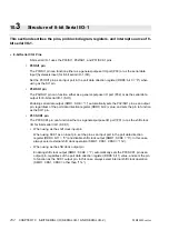
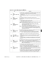
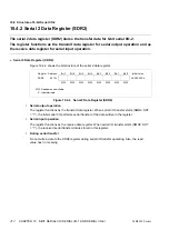
Table 10.3.1 Serial 1 Mode Register (SMR1) Bits
Bit
Function
Bit 7
SIOF:
Interrupt request flag
bit
• This bit is set to “1” when the serial output operation has output 8 bits of serial
data or the serial input operation has input 8 bits of serial data.
An interrupt request is output when both this bit and the interrupt request enable
bit (SIOE) are “1”.
• Writing “0” clears this bit. Writing “1” has no effect and does not change the bit
value.
Bit 6
SIOE:
Interrupt request
enable bit
This bit enables or disables an interrupt request output to the CPU. An interrupt
request is output when both this bit and the interrupt request flag bit (SIOF) are
“1”.
Bit 5
SCKE:
Shift clock output
enable bit
• This bit controls the shift clock input and output.
• The P31/SCK1 pin functions as the shift clock input pin when this bit is set to “0”
and as the shift clock output pin when set to “1”.
Check: • Set the P31/SCK1 pin as an input port when using this pin as the shift
clock input. Also, selects external shift clock operation in the shift clock
selection bits (CKS1, CKS0 = “11
B
”).
•
Select internal shift clock operation (CKS1, CKS0 = other than “11
B
”)
when using this pin as a shift clock output (SCKE = “1”).
Notes: • The pin functions as the SCK1 output pin when shift clock is enabled
(SCKE = “1”), regardless of the state of the general-purpose port (P31).
• Set to shift clock input operation (SCKE = “0”) when using this pin as a
general-purpose port (P31).
Bit 4
SOE:
Serial data output
enable bit
The P32/SO1 pin functions as a general-purpose port (P32) when this bit is set to
“0” and as the serial data output pin (SO1) when set to “1”.
Note: The pin functions as the SO1 pin when serial data output is enabled (SOE=
“1”), regardless of the state of the general-purpose port (P32).
Bit 3
Bit 2
CKS1, CKS0:
Shift clock selection
bits
• These bits select the shift clock from one external and three internal shift
clocks.
•
Setting these bits to other than “11
B
” selects an internal
shift clock. In this case,
the shift clock is output from the SCK1 pin if the shift clock output enable bit
(SCKE) is “1”.
•
Setting these bits to “11
B
” selects the external shift clock.
This inputs the shift
clock from the SCK1 pin if shift clock input is enabled (SCKE = “0” and DDR3:
bit 1 = “0”).
Bit 1
BDS:
Transfer direction
selection bit
This bit selects whether serial data is transferred with the least significant bit first
(LSB first, BDS = “0”) or the most significant bit first (MSB first, BDS = “1”).
Check: As bits are set in the appropriate order when writing to or reading from the
serial 1 data register (SDR1), modifying this bit does not apply to any data
already set in the SDR1 register.
Bit 0
SST:
Serial I/O transfer
start bit
• This bit controls serial I/O transfer start and transfer enable. This bit can also be
used to determine whether transfer has completed.
•
Writing “1” to this bit when an internal shift clock is selected (CKS1, CKS0 =
other than “11
B
”) clears the shift clock counter and starts data transfer.
• Writing “1” to this bit when
an external shift clock is selected (CKS1, CKS0 =
“11
B
”) enables data transfer, clears
the shift clock counter, and sets serial I/O-1
to delay for input of the external shift clock.
• This bit is cleared to “0” and the SIOF bit set to “1” when transfer completes.
• Writing “0” to this bit while transfer is in progress (SST = “1”) aborts the transfer.
After halting a transfer, data must be set again to the SDR register for data
output and transfer restarted (the shift clock counter cleared) for data input.
Содержание F2MC-8L MB89620 Series
Страница 8: ......
Страница 10: ...MB89620 series ...
Страница 11: ...vi MB89620 series ...
Страница 17: ...xii MB89620 series ...
Страница 18: ...xvi MB89620 series ...
Страница 30: ...MB89620 series CHAPTER 1 OVERVIEW 9 Memo ...
Страница 34: ...MB89620 series CHAPTER 1 OVERVIEW 13 Memo ...
Страница 42: ...MB89620 series CHAPTER 1 OVERVIEW 21 Memo ...
Страница 49: ...28 CHAPTER 1 OVERVIEW MB89620 series ...
Страница 62: ...MB89620 series CHAPTER 3 CPU 41 Memo ...
Страница 78: ...MB89620 series CHAPTER 3 CPU 57 Memo ...
Страница 82: ...MB89620 series CHAPTER 3 CPU 61 Memo ...
Страница 86: ...MB89620 series CHAPTER 3 CPU 65 Memo ...
Страница 90: ...MB89620 series CHAPTER 3 CPU 69 Memo ...
Страница 96: ...MB89620 series CHAPTER 3 CPU 75 Memo ...
Страница 122: ...MB89620 series CHAPTER 4 I O PORTS 101 Memo ...
Страница 144: ...MB89620 series CHAPTER 5 TIMEBASE TIMER 123 Memo ...
Страница 149: ...128 CHAPTER 5 TIMEBASE TIMER MB89620 series ...
Страница 157: ...136 CHAPTER 6 WATCHDOG TIMER MB89620 series ...
Страница 174: ...MB89620 series CHAPTER 7 8 BIT PWM TIMER 153 Memo ...
Страница 177: ...156 CHAPTER 7 8 BIT PWM TIMER MB89620 series ...
Страница 202: ...MB89620 series CHAPTER 9 16 BIT TIMER COUNTER 181 Memo ...
Страница 217: ...196 CHAPTER 9 16 BIT TIMER COUNTER MB89620 series ...
Страница 220: ...MB89620 series CHAPTER 10 8 BIT SERIAL I O SERIAL I O 1 AND SERIAL I O 2 199 Memo ...
Страница 228: ...MB89620 series CHAPTER 10 8 BIT SERIAL I O SERIAL I O 1 AND SERIAL I O 2 207 Memo ...
Страница 245: ...224 CHAPTER 10 8 BIT SERIAL I O SERIAL I O 1 AND SERIAL I O 2 MB89620 series ...
Страница 266: ...MB89620 series CHAPTER 13 A D CONVERTER 245 13 Memo ...
Страница 283: ...262 CHAPTER 13 A D CONVERTER MB89620 series ...
Страница 289: ...268 CHAPTER 14 CLOCK MONITOR FUNCTION MB89620 series ...
Страница 306: ...MB89620 series APPENDIX 285 APPEND Memo ...
Страница 319: ...298 APPENDIX MB89620 series Memo ...
Страница 321: ...2 ...
Страница 354: ......

