80
CHAPTER 3 CPU
MB89620 series
3.8 Memory Access Modes
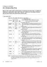
3.8.2 External Bus Pins
External bus mode must be allowed when connecting external memory or peripheral
functions. In external bus mode, port 0 and port 1 function as the external bus pins
and port 2 functions as the external bus control pins.
n
External Bus Pins
Check: •
In external bus mode, signals are output on the AD0 to AD7, A08 to A15, ALE, and CLK pins
even when accessing an internal area. However, the RD, WR, and BUFC pins go to the “H” level.
•
The HRQ, HAK, and BUFC pins can be set as output ports by the external bus pin control
register (BCTR).
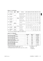
Table 3.8.2 External Bus Pin Functions in Each Mode
Pin name
Memory access mode
Single-chip mode
External ROM mode or internal ROM/external bus mode
Pin
name
Function
Pin
name
Function when external bus is operating
P00/AD0 to
P07/AD7
P00 to
P07
Port 0
General-
purpose
I/O ports
AD0
to AD7
Address/data multiplex bus I/O
These external bus pins are multiplexed in the time domain to act as
both the output for the lower 8 bits of the address and the data input and
output. The lower address must be latched externally using the ALE
signal.
P10/A08
to P17/A15
P10 to
P17
Port 1
General-
purpose
I/O ports
A08 to
A15
Address bus output
External bus pins that output the upper 8 bits of the address. Latching is
not required, as the output is maintained when the lower address is
multiplexed with data.
P20/BUFC
P20
Port 2
Output-only
ports
BUFC
Buffer control output
The signal controls the I/O direction for the external data bus buffer. An
“H” level indicates the output (write) direction and an “L” level indicates
the input (read) direction.
P21/
HAK
P21
HAK
Hold acknowledge output
The signal indicates that the CPU has released the external bus in
response to a hold request input (HRQ) from an external peripheral
function. An “L” level indicates that the external peripheral function can
use the bus.
P22/HRQ
P22
HRQ
Hold request input
The signal requests the CPU to release the external bus so that the bus
can be used by an external peripheral function. The external bus pins
and some external bus control pins go to the high-impedance state while
an “H” level is input to this pin.
P23/RDY
P23
RDY
Ready input
The signal is used to extend the bus cycle when accessing low-speed
external memory or other low-speed external devices. The bus cycle is
extended in the CPU operating clock units while an “L” level is input to
this pin. An external pull-up must be provided for this pin if the ready
function is not used.
P24/CLK
P24
CLK
Clock output
Outputs the CPU operating clock. The CPU operates in sync with this
clock. This divide-by-two clock (divide-by-four source oscillation) is
called the instruction cycle or the bus cycle.
P25/
WR
P25
WR
Write strobe output
Strobe signal for writing data. During a write operation, the pin goes to
the “L” level and the data is output on the data bus. The write destination
reads the data off the data bus on the rising edge of this signal.
P26/
RD
P26
RD
Read strobe output
Strobe signal for reading data. During a read operation, the pin goes to
the “L” level and the data is read from the data bus on the rising edge.
P27/ALE
P27
ALE
Address latch enable output
This signal is used to externally latch the lower address. Connect a latch
that holds the address on the falling edge of this signal.
Содержание F2MC-8L MB89620 Series
Страница 8: ......
Страница 10: ...MB89620 series ...
Страница 11: ...vi MB89620 series ...
Страница 17: ...xii MB89620 series ...
Страница 18: ...xvi MB89620 series ...
Страница 30: ...MB89620 series CHAPTER 1 OVERVIEW 9 Memo ...
Страница 34: ...MB89620 series CHAPTER 1 OVERVIEW 13 Memo ...
Страница 42: ...MB89620 series CHAPTER 1 OVERVIEW 21 Memo ...
Страница 49: ...28 CHAPTER 1 OVERVIEW MB89620 series ...
Страница 62: ...MB89620 series CHAPTER 3 CPU 41 Memo ...
Страница 78: ...MB89620 series CHAPTER 3 CPU 57 Memo ...
Страница 82: ...MB89620 series CHAPTER 3 CPU 61 Memo ...
Страница 86: ...MB89620 series CHAPTER 3 CPU 65 Memo ...
Страница 90: ...MB89620 series CHAPTER 3 CPU 69 Memo ...
Страница 96: ...MB89620 series CHAPTER 3 CPU 75 Memo ...
Страница 122: ...MB89620 series CHAPTER 4 I O PORTS 101 Memo ...
Страница 144: ...MB89620 series CHAPTER 5 TIMEBASE TIMER 123 Memo ...
Страница 149: ...128 CHAPTER 5 TIMEBASE TIMER MB89620 series ...
Страница 157: ...136 CHAPTER 6 WATCHDOG TIMER MB89620 series ...
Страница 174: ...MB89620 series CHAPTER 7 8 BIT PWM TIMER 153 Memo ...
Страница 177: ...156 CHAPTER 7 8 BIT PWM TIMER MB89620 series ...
Страница 202: ...MB89620 series CHAPTER 9 16 BIT TIMER COUNTER 181 Memo ...
Страница 217: ...196 CHAPTER 9 16 BIT TIMER COUNTER MB89620 series ...
Страница 220: ...MB89620 series CHAPTER 10 8 BIT SERIAL I O SERIAL I O 1 AND SERIAL I O 2 199 Memo ...
Страница 228: ...MB89620 series CHAPTER 10 8 BIT SERIAL I O SERIAL I O 1 AND SERIAL I O 2 207 Memo ...
Страница 245: ...224 CHAPTER 10 8 BIT SERIAL I O SERIAL I O 1 AND SERIAL I O 2 MB89620 series ...
Страница 266: ...MB89620 series CHAPTER 13 A D CONVERTER 245 13 Memo ...
Страница 283: ...262 CHAPTER 13 A D CONVERTER MB89620 series ...
Страница 289: ...268 CHAPTER 14 CLOCK MONITOR FUNCTION MB89620 series ...
Страница 306: ...MB89620 series APPENDIX 285 APPEND Memo ...
Страница 319: ...298 APPENDIX MB89620 series Memo ...
Страница 321: ...2 ...
Страница 354: ......

