MB89620 series
CHAPTER 4 I/O PORTS
107
4.5 Port 4
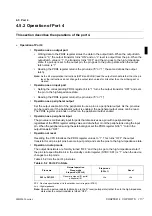
4.5.2 Operation of Port 4
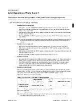
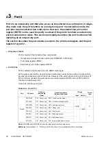
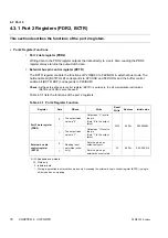
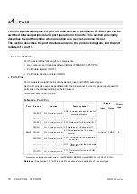
This section describes the operations of the port 4.
n
Operation of Port 4
l
Operation as an output port
•
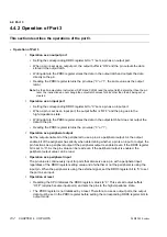
Writing data to the PDR4 register stores the data in the output latch. When the output latch
value is “0,” the output transistor turns “ON” and an “L” level is output from the pin. When the
output latch value is “1”, the transistor turns “OFF” and the pin goes to the high-impedance
state. If a pull-up is set to the output pin, the pin goes to the pull-up state when the output
latch value is “1”.
•
Reading the PDR4 register returns the pin value (“0” or “1”, the same data as the output
latch).
Note:
As the bit manipulation instructions (SETB and CLRB) read the output latch data rather than the pin
level, the instructions do not change the output latch values for bits other than the bit being set or
cleared.
l
Operation as an input port
•
Setting the corresponding PDR4 register bit to “1” turns the output transistor “OFF” and sets
the pin to the high-impedance state.
•
Reading the PDR4 register returns the pin value (“0” or “1”).
l
Operation as a peripheral output
Set the output enable bit of the peripheral to use a pin as a peripheral output. As the pin value
can be read even if the peripheral output is enabled, the peripheral output value can be read.
The PDR4 register value has no effect on the peripheral output enable.
l
Operation as a peripheral input
The pin value is continuously input for ports that also serves as a pin with a peripheral input,
regardless of the PDR4 register setting value and of whether or not the peripheral is using the input
pin. When the peripheral is using the external signal, set the PDR4 register bit to “1” to turn the
output transistor “OFF”.
l
Operation at reset
Resetting the CPU initializes the PDR4 register values to “1”. This turns “OFF” the output
transistor for all pins (all pins become input ports) and sets the pins to the high-impedance state.
l
Operation in stop mode
The output transistors are forcibly turned “OFF” and the pins go to the high-impedance state if
the pin state specification bit in the standby control register (STBC: SPL) is “1” when the device
changes to stop mode.
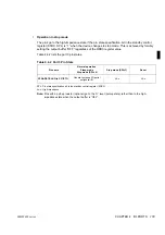
Table 4.5.2 lists the port 4 pin states.
SPL : Pin state specification bit in the standby control register (STBC)
Hi-z : High impedance
Note:
Pins with a pull-up resistor (optional) go to the “H” level (pull-up state) rather than to the high-impedance
state when the output transistor is turned “OFF”.
Table 4.5.2 Port 4 Pin State
Pin name
Normal operation
Sleep mode
Stop mode (SPL=0)
Stop mode
(SPL=1)
Reset
P40 to P47/SI2
General-purpose I/O ports/
peripheral I/O
Hi-z
Hi-z
Содержание F2MC-8L MB89620 Series
Страница 8: ......
Страница 10: ...MB89620 series ...
Страница 11: ...vi MB89620 series ...
Страница 17: ...xii MB89620 series ...
Страница 18: ...xvi MB89620 series ...
Страница 30: ...MB89620 series CHAPTER 1 OVERVIEW 9 Memo ...
Страница 34: ...MB89620 series CHAPTER 1 OVERVIEW 13 Memo ...
Страница 42: ...MB89620 series CHAPTER 1 OVERVIEW 21 Memo ...
Страница 49: ...28 CHAPTER 1 OVERVIEW MB89620 series ...
Страница 62: ...MB89620 series CHAPTER 3 CPU 41 Memo ...
Страница 78: ...MB89620 series CHAPTER 3 CPU 57 Memo ...
Страница 82: ...MB89620 series CHAPTER 3 CPU 61 Memo ...
Страница 86: ...MB89620 series CHAPTER 3 CPU 65 Memo ...
Страница 90: ...MB89620 series CHAPTER 3 CPU 69 Memo ...
Страница 96: ...MB89620 series CHAPTER 3 CPU 75 Memo ...
Страница 122: ...MB89620 series CHAPTER 4 I O PORTS 101 Memo ...
Страница 144: ...MB89620 series CHAPTER 5 TIMEBASE TIMER 123 Memo ...
Страница 149: ...128 CHAPTER 5 TIMEBASE TIMER MB89620 series ...
Страница 157: ...136 CHAPTER 6 WATCHDOG TIMER MB89620 series ...
Страница 174: ...MB89620 series CHAPTER 7 8 BIT PWM TIMER 153 Memo ...
Страница 177: ...156 CHAPTER 7 8 BIT PWM TIMER MB89620 series ...
Страница 202: ...MB89620 series CHAPTER 9 16 BIT TIMER COUNTER 181 Memo ...
Страница 217: ...196 CHAPTER 9 16 BIT TIMER COUNTER MB89620 series ...
Страница 220: ...MB89620 series CHAPTER 10 8 BIT SERIAL I O SERIAL I O 1 AND SERIAL I O 2 199 Memo ...
Страница 228: ...MB89620 series CHAPTER 10 8 BIT SERIAL I O SERIAL I O 1 AND SERIAL I O 2 207 Memo ...
Страница 245: ...224 CHAPTER 10 8 BIT SERIAL I O SERIAL I O 1 AND SERIAL I O 2 MB89620 series ...
Страница 266: ...MB89620 series CHAPTER 13 A D CONVERTER 245 13 Memo ...
Страница 283: ...262 CHAPTER 13 A D CONVERTER MB89620 series ...
Страница 289: ...268 CHAPTER 14 CLOCK MONITOR FUNCTION MB89620 series ...
Страница 306: ...MB89620 series APPENDIX 285 APPEND Memo ...
Страница 319: ...298 APPENDIX MB89620 series Memo ...
Страница 321: ...2 ...
Страница 354: ......

