


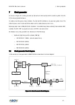


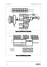
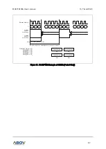


7. Clock generator
MC97F6108A User’s manual
76
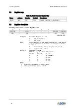
7.2
Register map
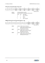
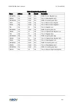
Table 10. Clock Generator Register Map
Name
Address
Direction
Default
Description
SCCR
8AH
R/W
00H
System and Clock Control Register
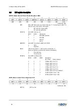
7.3
Register description
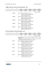
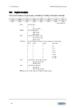
SCCR (System and Clock Control Register): 8AH
7
6
5
4
3
2
1
0
WDTRCON
–
CHBS
–
–
–
SYSCLK1
SYSCLK0
R/W
–
R/W
–
–
–
R/W
R/W
Initial value: 00H
WDTRCON
Select WDTRC oscillator on or off.
0
WDTRC off (default)
1
WDTRC on
CHBS
Control the scheme of clock change. If this bit set to
‘0’, clock change is
controlled by hardware. But if this set to
‘1’, clock change is controlled by
software.
0
Clock changed by hardware during stop mode (default)
1
Clock changed by software
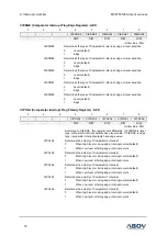
SYSCK[1:0]
Determine division rate.
NOTE:
To change by software, CHBS set to
‘1’
SYSCK1
SYSCK0
Description
0
0
fINTRC(default)
0
1
fINTRC/2
1
0
fINTRC/4
1
1
fINTRC/8
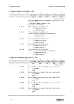
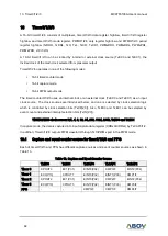
NOTES
:
1.
SCCR[2], SCCR[3] and SCCR[4] must be kept '0'.
2.
When clear CHBS, keep other bits in SCCR.