


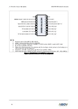


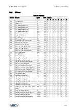
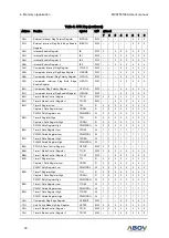


2. Pinouts and pin description
MC97F6108A User’s manual
18
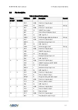
Table 2. Normal Pin Description (continued)
Pin no.
PIN Name
I/O
(1)
Description
Remark
20 SOP
16 SOPN
10
-
T2O
O
Timer 2 interval output
AN6
IA
ADC input ch-6
11
-
P11*
IOUS
Port 1 bit 1 Input/output
DSCL1
IOU
OCD debugger clock
Pull-up
12
-
P12*
IOUS
Port 1 bit 2 Input/output
DSDA1
IOU
OCD debugger data input/output
Pull-up
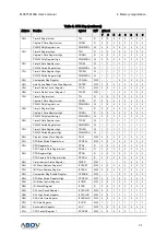
13
9
P13*
IOUS
Port 1 bit 3 Input/output
CMP1_IN_P
IUS
Comparator1 input positive signal
14
10
P14*
IOUS
Port 1 bit 4 Input/output
CMP2_IN_P
IUS
Comparator2 input positive signal
15
11
P15*
IOUS
Port 1 bit 5 Input/output
CMP0_IN_P
IUS
Comparator0 input positive signal
16
12
P16*
IOUS
Port 1 bit 6 Input/output
CMP0_IN_N
IUS
Comparator0 input negative signal
17
13
P17*
IOUS
Port 1 bit 7 Input/output
AN7
IA
ADC input ch-7
AVREF
P
A/D converter reference voltage
(AMP1O)
O
OP-AMP 1 output
18
14
P20*
IOUS
Port 2 bit 0 Input/output
AN5
IA
ADC input ch-5
AMP2O
O
OP-AMP 2 output
19
15
P21*
IOUS
Port 2 bit 1 Input/output
AMP1I
I
OP-AMP 1 input
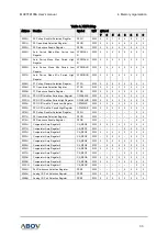
1
1
VDD
P
VDD
20
16
VSS
P
VSS
NOTES
:
1.
P00 and P10–P12 are not in the 16-pin package.
2.
P00/RSTB pin is configured as one of the P00 and RESETB pin by the “CONFIGURE OPTION.”
3.
If the P01/XCK/EC1/AN0/DSDA and P02/EINT0/AN1/DSCL pins are connected to the programmer
during power-on reset, the pins are automatically configured as In-system programming pins.
4.
Or if the P11/DSCL1 and P12/DSDA1 pins are connected to the programmer during power-on reset, the
pins are automatically configured as In-system programming pins.
5.
P01/XCK/EC1/AN0/DSDA, P02/EINT0/AN1/DSCL, P11/DSCL1 and P12/DSDA1 pins are only
configured as inputs with internal pull-up resistor during the reset or power-on reset.
(1)
I=Input, O=Output, U=Pull-up, D=Pull-down, S=Schmitt-Trigger Input Type, C=CMOS Input Type,
A=Analog, P=Power
6.
The * means ‘Selected pin function after reset condition.