


MC97F6108A User’s manual
2. Pinouts and pin description
15
2
Pinouts and pin description
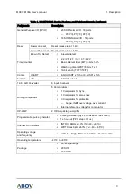
In this chapter, MC97F6108A device pinouts and pin descriptions are introduced.
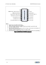
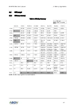
2.1
Pinouts
MC
97
F6
10
8AD
1
2
3
4
5
6
7
8
9
10
20
19
18
17
16
15
14
13
12
11
VDD
RESETB/P00
DSDA
/AN0/EC1/CMPXO/SCK/XCK/P01
DSCL
/AN1/EINT0/SS/P02
AN2/EINT1/SDA/MISO/RXD/P03
AN3/EINT2/SCL/MOSI/TXD/P04
PPGO/PWM3O/T3O/P05
AN4/PWM1O/T1O/P06
TPPGO/BUZO/PWM0O/T0O/P07
AN6/PWM2O/T2O/EC0/P10
VSS
P21/AMP1I
P20/AN5/AMP2O
P17/AN7/AVREF/(AMP1O)
P16/CMP0_IN_N
P15/CMP0_IN_P
P14/CMP2_IN_P
P13/CMP1_IN_P
P12/
DSDA1
P11/
DSCL1
NOTES
:
1.
Monitor function: P01/CMPXO, P07/TPPGO
2.
USART function: P01/XCK, P04/TXD, P03/RXD
3.
SPI function: P02/SS, P04/MOSI, P03/MISO, P01/SCK (when USART is used as SPI mode)
4.
I2C function: P03/SDA, P04/SCL
5.
When using 16-pin products, it is recommended that configure internal pull-up to the floating pin in
order to prevent current consumption.
6.
Programmer (E-PGM+, E-Gang4/6) uses P0[1:2] or P1[1:2] pin as DSCL/DSCL1, DSDA/DSDA1.
7.
The second functions of DSDA and DSCL port are not supported in OCD mode. (EC1, XCK, EINT0).
Figure 2. MC97F6108A 20 SOP Pin Assignment