


MC97F6108A User’s manual
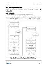
19. Memory programming
205
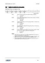
FEDR (Flash Data Register): F5H
7
6
5
4
3
2
1
0
FEDR7
FEDR 6
FEDR 5
FEDR 4
FEDR 3
FEDR 2
FEDR 1
FEDR 0
W
W
W
W
W
W
W
W
Initial value: 00H
FEDR[7:0]
Flash and EEPROM data
NOTES
:
1.
Data register. In no program/erase/verify mode, READ/WRITE of FECR bits read
or write data from FLASH to this register or from this register to Flash.
2.
The mode entrance sequence is to write 0xA5 and 0x5A to it in order.
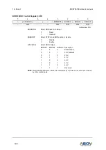
FETCR (Flash Time control Register): EDH
7
6
5
4
3
2
1
0
TCR7
TCR6
TCR5
TCR4
TCR3
TCR2
TCR1
TCR0
R/W
R/W
R/W
R/W
R/W
R/W
R/W
R/W
Initial value: 00H
TCR[7:0]
Flash Time control
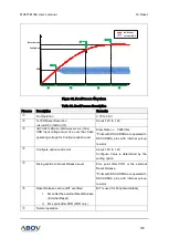
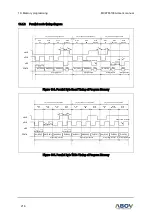
Program and erase time is controlled by setting FETCR register. Program and erase timer uses 10-bit counter. It
increases by one at each the divided system clock frequency (=SCLK/128).
It is cleared when program or erase starts. Timer stops when 10-bit counter is same to FETCR. PEVBSY is cleared
when program, erase or verify starts and set when program, erase or verify stops.
Max program/erase time at 16MHz system clock : (255+1) * 2 * (62.5ns * 128) = 4.096ms
In the case of
±
10% of error rate of counter source clock, program or erase time is 3.6~4.5ms.
* Program/erase time calculation:
For page write or erase = Tpe = (TCON+1) * 2 * (T
SCLK
*128)
For bulk erase, Tbe = (TCON+1) * 4 * (T
SCLK
*128)
Recommended bulk erase time :
FETCR = 4Eh
Recommended program / page erase time :
FETCR = 9Dh
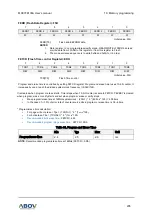
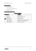
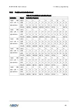
Table 31. Program and Erase Time
Min
Typ
Max
Unit
Program/erase time
2.4
2.5
2.6
ms
NOTE
: Recommended program/erase time at 16MHz (FETCR = 9Dh)