


14. 12-bit AD Converter (ADC)
MC97F6108A User’s manual
140
14
12-bit AD Converter (ADC)
Analog-to-digital converter (ADC) of MC97F6108A allows conversion of an analog input signal to
corresponding 12-bit digital value. This A/D module has eight analog inputs. Output of the multiplexer
becomes input into the converter which generates the result through successive approximation.
The A/D module has four registers which are the A/D converter mode register (ADCM), A/D converter
mode register1 (ADCM1), A/D converter result high register (ADCRH), and A/D converter result low
register (ADCRL).
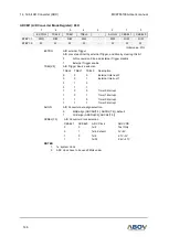
ADSEL[3:0] bits are used to select channels to be converted. To execute A/D conversion, ADST bit
should be set to ‘
1
’. Registers ADC
RH and ADCRL contain the result of A/D conversion. When the
conversion is completed, the result is loaded into ADCRH and ADCRL, A/D conversion status bit
AFLAG is set to ‘1’, and A/D interrupt is set. During the A/D conversion, AFLAG bit is read as ‘0’.
If
STBY (power down) bit is used, the ADC is disabled. Also interrupt of internal timer, external event
counter can start A/D conversion regardless of interrupt occurrence.
14.1
Conversion timing
A/D conversion process requires 4 steps (4 clock edges) to convert each bit and 12 clocks to set up
A/D conversion. Therefore, total of 58 clocks are required to complete a 12-bit conversion: For example,
when fxx/8 is selected for conversion clock with a 12MHz fxx clock frequency, one clock cycle is 0.66μs,
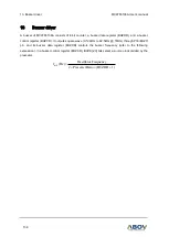
and each bit conversion requires 4 clocks. The conversion rate is calculated as follows:
4 clocks/bit × 12 bits +
set-up time = 60 clocks
ADC Conversion Time = ADCLK * 60 cycles
ADC clock have to be used under 3MHz. So remember that the A/D converter requires at least 20us
for conversion time, so the conversion time must be set bigger than or equal to 20us.
NOTE:
When the A/D conversion is used, the port direction register to be used is set to input mode (PxIO).
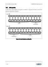
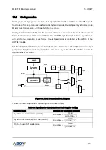
14.2
Block diagram
In this section, the 12-bit ADC is described in a block diagram, and an analog input pin and a power pin
with capacitors respectively are introduced.