

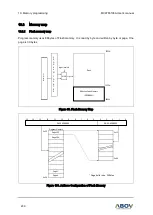
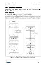


19. Memory programming
MC97F6108A User’s manual
216
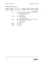
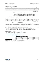
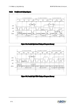
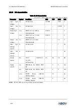
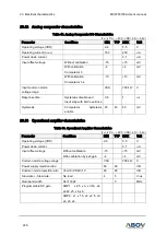
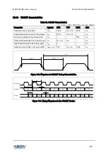
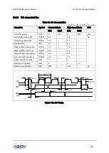
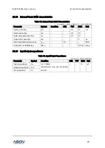
19.4.2
Parallel mode timing diagram
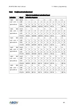
Figure 104. Parallel Byte Read Timing of Program Memory
Figure 105. Parallel Byte Write Timing of Program Memory
nALE
nWR
nRD
PDATA
Read @0F000H
AM(F0H)
AL(00H)
DO
Read @0A000H
AM(A0H)
AL(00H)
AL(01H)
DO
Read @0A001H
Write
Write
Write
Read
Write
Write
Read
Write
T
AS
T
AH
Read
address auto-
increment
AH(00H)
DO
Read
AL
AM
AH
Data Out
AL
AM
Data Out
AL
Data Out
Data Out
DO
1
-
byte read with 3
1
-
byte read with 2
-byte address
2
-
byte read with 1
-byte address
T
OA
Read @0A002H
T
RL
T
RH
T
AWS
T
AWH
T
ARS
T
ARH
-byte address
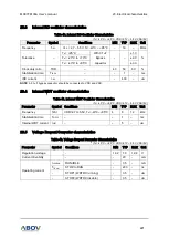
nWR
nRD
PDATA
Write 0x00 @0x0F000
AM(F0H)
AL(00H)
Write 0x01 @0x0A000H
AM(A0H)
AL(00H)
AL(01H)
Write 0x02 @0x0A001
Write
Write
Write
Write
Write
Write
Write
Write
T
AS
T
AH
T
WE
Read
address auto-
-
increment
AH(00H)
Write
AL
AM
AH
Data
AL
AM
Data
AL
Data Out
Data
1
-
byte write with 3
-
byte address
1
-
byte write with 2
-
byte address
2
-
byte write with 1
-
byte address
Write 0x03 @0x0A002
DI(00H)
DI(01H)
DI(02H)
DI(03H)
T
WH
nALE
T
DH
T
DS
T
AWS
T
AWH