


MC97F6108A User’s manual
15. USART
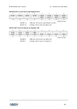
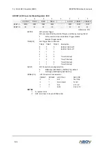
159
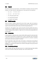
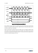
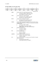
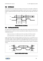
Figure 74. SPI Clock Formats when UCPHA = 1
When UCPHA=1, the slave begins to drive its MISO output when SS goes active low, but the data is
not defined until the first XCK edge. The first XCK edge shifts the first bit of data from the shifter onto
the MOSI output of the master and the MISO output of the slave.
The next XCK edge causes both the master and the slave to sample the data bit value on their MISO
and MOSI inputs, respectively.
At the third XCK edge, USART shifts the second data bit value out to the MOSI and MISO output of the
master and slave respectively. When UCPHA=1, the slave’s SS input is not req
uired to go to its inactive
high level between transfers.
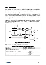
Because an SPI logic reuses USART resources, SPI mode of operation is similar to that of synchronous
or asynchronous operation. An SPI transfer is initiated by checking for USART Data Register Empty
flag (UDRE=1) and then by writing a byte of data to the UDATA Register.
In master mode of operation, even if transmission is not enabled (TXE=0), writing data to UDATA
register is necessary because the clock XCK is generated from a transmitter block.
XCK
(UCPOL=1)
MISO2
MOSI2
XCK
(UCPOL=0)
/SS2 OUT
(MASTER)
BIT7
BIT0
/SS2 IN
(SLAVE)
BIT6
BIT1
…
…
BIT2
BIT5
BIT0
BIT7
BIT1
BIT6
SAMPLE
MSB First
LSB First