


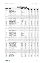

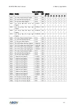


MC97F6108A User’s manual
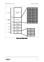
4. Memory organization
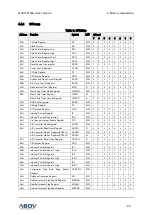
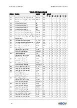
35
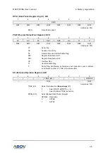
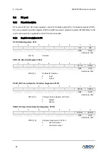
DPH1 (Data Pointer Register High 1): 85H
7
6
5
4
3
2
1
0
DPH1
R/W
R/W
R/W
R/W
R/W
R/W
R/W
R/W
Initial value: 00H
DPH1
Data Pointer High 1
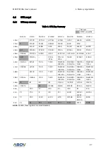
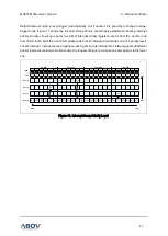
PSW (Program Status Word Register): D0H
7
6
5
4
3
2
1
0
CY
AC
F0
RS1
RS0
OV
F1
P
R/W
R/W
R/W
R/W
R/W
R/W
R/W
R/W
Initial value: 00H
CY
Carry Flag
AC
Auxiliary Carry Flag
F0
General Purpose User-Definable Flag
RS1
Register Bank Select bit 1
RS0
Register Bank Select bit 0
OV
Overflow Flag
F1
User-Definable Flag
P
Parity Flag. Set/Cleared by hardware each instruction cycle to indicate
an odd/even number of ‘1’ bits in the accumulator
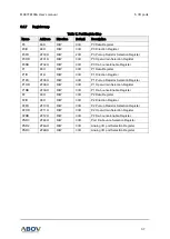
EO (Extended Operation Register): A2H
7
6
5
4
3
2
1
0
–
–
–
TRAP_EN
–
–
–
DPSEL0
–
–
–
R/W
–
–
–
R/W
Initial value: 00H
TRAP_EN
Select the Instruction
(Keep always ‘0’)
.
0
Select MOVC @(DPTR++), A
1
Select Software TRAP Instruction
DPSEL[2:0]
Select Banked Data Pointer Register
DPSEL0 Description
0
DPTR0
1
DPTR1