S
Device Addr
Wr
A
Command
A
Sr
Device Addr
Rd
A
Byte Count = N
A
Byte #0
A
……
Byte #(N-1)
A
PEC
NA
P
S
Device Addr
Wr
A
Command
A
Sr
Device Addr
Rd
A
Byte Count = N
A
Byte #0
A
……
Byte #(N-1)
NA
P
Master Mode Operation Reference
378
SNIU028A – February 2016 – Revised April 2016
Copyright © 2016, Texas Instruments Incorporated
PMBus Interface/I2C Interface
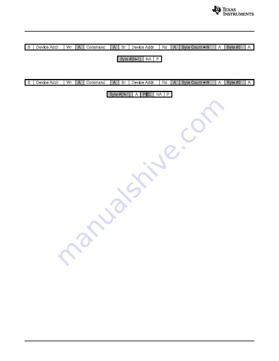
10.7.8 Block Read
Figure 10-39. Block Read w/o PEC Byte
Figure 10-40. Block Read with PEC Byte
The Block Read protocol is similar to a Read Word in its structure, with the exception of reception of more
than 2 data bytes from the Slave. The first data byte transmitted by the Slave represents the block length
of the data being written by the slave. If PEC processing is enabled, the Slave appends a PEC byte to the
end of the message.
To initiate a Block Read message on the PMBus, the Master Control Register is programmed with the
block length in the Byte Count bits. This count excludes the command byte, any slave address and the
block length bytes in the message. The command byte to be transmitted to the Slave is written into bits 7-
0 of the Transmit Data Register prior to the programming of the Master Control Register.
After configuring the Master Control Register, the Block Read message is initiated on the PMBus. The
interface interrupts the firmware upon receipt of 4 data bytes from the slave. If the block length is 3, the
EOM interrupt will be received concurrently with the data ready interrupt. Otherwise, a data ready interrupt
is asserted, indicating 4 bytes are ready for reading by the firmware. At the end of the message, less than
4 bytes may be stored in the Receive Data Register. The RX Byte Count bits in the Status Register
indicate the number of bytes available in the final data transfer. The firmware may verify the received PEC
upon detection of the End of Message interrupt.


