


General-purpose timers (TIM15/TIM16/TIM17)
RM0351
1078/1830
DocID024597 Rev 5
Break events can also be generated by software using BG bit in the TIMx_EGR register.
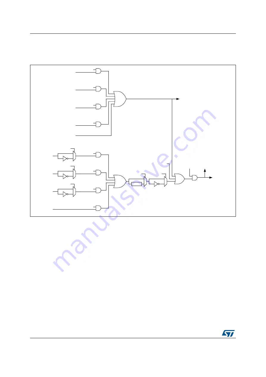
All sources are ORed before entering the timer BRK inputs, as per
below.
Figure 346. Break circuitry overview
Note:
An asynchronous (clockless) operation is only guaranteed when the programmable filter is
disabled. If it is enabled, a fail safe clock mode (for example by using the internal PLL and/or
the CSS) must be used to guarantee that break events are handled.
When a break occurs (selected level on the break input):
•
The MOE bit is cleared asynchronously, putting the outputs in inactive state, idle state
or even releasing the control to the AFIO controller (selected by the OSSI bit). This
feature functions even if the MCU oscillator is off.
•
Each output channel is driven with the level programmed in the OISx bit in the
TIMx_CR2 register as soon as MOE=0. If OSSI=0, the timer releases the output control
(taken over by the AFIO controller) else the enable output remains high.
•
When complementary outputs are used:
–
The outputs are first put in reset state inactive state (depending on the polarity).
This is done asynchronously so that it works even if no clock is provided to the
timer.
–
If the timer clock is still present, then the dead-time generator is reactivated in
order to drive the outputs with the level programmed in the OISx and OISxN bits
after a dead-time. Even in this case, OCx and OCxN cannot be driven to their
06Y9
&203RXWSXW
')6'0
%5($.RXWSXW
%.')%.[(
%.&03(
%.&033
&203RXWSXW
%.&03(
%.&033
%.,1LQSXWV
IURP$)
FRQWUROOHU
%.,1(
%.,13
%.)>@
)LOWHU
%.3
6RIWZDUHEUHDNUHTXHVWV%*
%.(
$SSOLFDWLRQEUHDNUHTXHVWV
%5.UHTXHVW
(&&/2&.
3DULW\/2&.
39'/2&.
/RFNXS/2&.
(&&(UURU
5$0SDULW\(UURU
39'
&RUH/RFNXS
&66
%,)IODJ
6%,)IODJ
6\VWHPEUHDNUHTXHVWV