


Serial Communication Interface (S12SCIV6)
MC9S12VRP Family Reference Manual Rev. 1.3
NXP Semiconductors
307
10.3.2.2
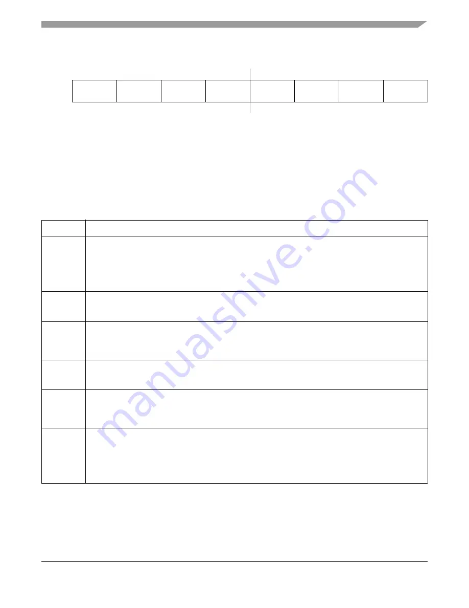
SCI Control Register 1 (SCICR1)
Read: Anytime, if AMAP = 0.
Write: Anytime, if AMAP = 0.
NOTE
This register is only visible in the memory map if AMAP = 0 (reset
condition).
7
6
5
4
3
2
1
0
R
LOOPS
SCISWAI
RSRC
M
WAKE
ILT
PE
PT
W
Reset
0
0
0
0
0
0
0
0
Figure 10-5. SCI Control Register 1 (SCICR1)
Table 10-3. SCICR1 Field Descriptions
Field
Description
7
LOOPS
Loop Select Bit
— LOOPS enables loop operation. In loop operation, the RXD pin is disconnected from the SCI
and the transmitter output is internally connected to the receiver input. Both the transmitter and the receiver must
be enabled to use the loop function.
0 Normal operation enabled
1 Loop operation enabled
The receiver input is determined by the RSRC bit.
6
SCISWAI
SCI Stop in Wait Mode Bit
— SCISWAI disables the SCI in wait mode.
0 SCI enabled in wait mode
1 SCI disabled in wait mode
5
RSRC
Receiver Source Bit
— When LOOPS = 1, the RSRC bit determines the source for the receiver shift register
input. See
.
0 Receiver input internally connected to transmitter output
1 Receiver input connected externally to transmitter
4
M
Data Format Mode Bit
— MODE determines whether data characters are eight or nine bits long.
0 One start bit, eight data bits, one stop bit
1 One start bit, nine data bits, one stop bit
3
WAKE
Wakeup Condition Bit
— WAKE determines which condition wakes up the SCI: a logic 1 (address mark) in the
most significant bit position of a received data character or an idle condition on the RXD pin.
0 Idle line wakeup
1 Address mark wakeup
2
ILT
Idle Line Type Bit
— ILT determines when the receiver starts counting logic 1s as idle character bits. The
counting begins either after the start bit or after the stop bit. If the count begins after the start bit, then a string of
logic 1s preceding the stop bit may cause false recognition of an idle character. Beginning the count after the
stop bit avoids false idle character recognition, but requires properly synchronized transmissions.
0 Idle character bit count begins after start bit
1 Idle character bit count begins after stop bit
Summary of Contents for MC9S12VRP64
Page 16: ...MC9S12VRP Family Reference Manual Rev 1 3 16 NXP Semiconductors ...
Page 46: ...Device Overview S12VRP Series MC9S12VRP Family Reference Manual Rev 1 3 46 NXP Semiconductors ...
Page 236: ...S12S Debug Module S12DBGV2 MC9S12VRP Family Reference Manual Rev 1 3 236 NXP Semiconductors ...
Page 244: ...Interrupt Module S12SINTV1 MC9S12VRP Family Reference Manual Rev 1 3 244 NXP Semiconductors ...
Page 358: ...Timer Module TIM16B2CV3 MC9S12VRP Family Reference Manual Rev 1 3 358 NXP Semiconductors ...
Page 436: ...Supply Voltage Sensor BATSV2 MC9S12VRP Family Reference Manual Rev 1 3 436 NXP Semiconductors ...
Page 528: ...NVM Electrical Parameters MC9S12VRP Family Reference Manual Rev 1 3 528 NXP Semiconductors ...
Page 530: ...Package Information MC9S12VRP Family Reference Manual Rev 1 3 530 NXP Semiconductors ...
Page 531: ...Package Information MC9S12VRP Family Reference Manual Rev 1 3 NXP Semiconductors 531 ...
Page 532: ...Package Information MC9S12VRP Family Reference Manual Rev 1 3 532 NXP Semiconductors ...


